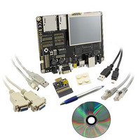
BMSKTOPASA900(DCE) Toshiba, BMSKTOPASA900(DCE) Datasheet - Page 431

BMSKTOPASA900(DCE)
Manufacturer Part Number
BMSKTOPASA900(DCE)
Description
KIT STARTER TMPA900 USB JTAG
Manufacturer
Toshiba
Series
TOPASr
Type
MCUr
Specifications of BMSKTOPASA900(DCE)
Contents
Evaluation Board, Cable(s), Software and Documentation
For Use With/related Products
TMPA900CMXBG
Lead Free Status / RoHS Status
Lead free / RoHS Compliant
- Current page: 431 of 959
- Download datasheet (5Mb)
[31:8]
[7:1]
[0]
[Description]
a. <SA[6:0]>
b. <ALS>
Bit
Writes to this register must be done before a start condition is generated or after a stop condition is generated. Writes
cannot be performed during transfer.
3.
that the master sends immediately after a start condition as a 7-bit address plus one
direction bit.
performed based on the free data format.
slave address set in I2C0AR<SA[6:0]>. If the 7-bit address matches the slave address, the
device uses the direction bit to determine whether to act as a transmitter or receiver. At
this time, if I2C0CR1<NOACK> = 0, the device pulls the SDA line low during the 9th
(acknowledge) clock output from the master.
a stop condition or a start condition by the restart procedure appears on the bus.
SDA line and SCL line high and does not participate in transfer operation until a stop
condition or a start condition by the restart procedure appears on the bus.
general call) and I2C0CR1<NOACK> = 0, the device returns an acknowledge signal and
acts as a slave receiver regardless of the slave address set in I2C0AR<SA[6:0]>.
operate as a slave device even if the 7-bit address matches the slave address or a general
call is detected.
the master as data and pulls the SDA line low during the 9th (acknowledge) clock output
from the master. Thereafter the device continues to perform receive operation as a slave
until a stop condition or a start condition by the restart procedure appears on the bus (free
format operation). In this case, the I2C0CR1<NOACK> value has no effect.
to be performed is determined by the 7-bit address (plus one direction bit) that the master
sends immediately after a start condition.
These bits are used to set the slave device address (7 bits) when this module is a slave.
When slave address recognition is enabled in I2C0AR<ALS>, the data transfer operation
This bit is used to enable or disable slave address recognition.
0y0: Enable (I
0y1: Disable (Free data format)
When this module is a slave, this bit specifies whether or not to recognize the 8-bit data
When <ALS> = 0, I
When <ALS> = 0, the device compares the 7-bit address sent from the master against the
Thereafter, the device continues to perform transmit or receive operation as a slave until
If the 7-bit address does not match the slave address, the device continues to leave the
If the 7-bit address plus one direction bit sent from the master are all 0s (indicating a
When I2C0CR1<NOACK> = 1, the device does not return any acknowledge signal nor
When <ALS> = 1, the device receives the 7-bit address plus one direction bit sent from
I2C0AR (I
−
SA[6:0]
ALS
Bit Symbol
2
C0 (Slave) Address Register)
2
C bus mode)
−
R/W
R/W
2
C bus mode is selected. When <ALS> = 1, transfer operation is
Type
TENTATIVE
TMPA900CM- 430
Undefined
0y0000000
0y0
Reset
Value
Read as undefined. Write as zero.
Set the slave address.
Address recognition enable/disable
0y0: Enable (I
0y1: Disable (Free data format)
Address = (0xF007_0000) + (0x0008)
2
C bus mode)
Description
TMPA900CM
2009-10-14
Related parts for BMSKTOPASA900(DCE)
Image
Part Number
Description
Manufacturer
Datasheet
Request
R
Part Number:
Description:
Toshiba Semiconductor [TOSHIBA IGBT Module Silicon N Channel IGBT]
Manufacturer:
TOSHIBA Semiconductor CORPORATION
Datasheet:
Part Number:
Description:
TOSHIBA GTR MODULE SILICON NPN TRIPLE DIFFUSED TYPE
Manufacturer:
TOSHIBA Semiconductor CORPORATION
Datasheet:
Part Number:
Description:
TOSHIBA GTR Module Silicon N Channel IGBT
Manufacturer:
TOSHIBA Semiconductor CORPORATION
Datasheet:
Part Number:
Description:
TOSHIBA Intelligent Power Module Silicon N Channel IGBT
Manufacturer:
TOSHIBA Semiconductor CORPORATION
Datasheet:
Part Number:
Description:
TOSHIBA INTELLIGENT POWER MODULE SILICON N CHANNEL LGBT
Manufacturer:
TOSHIBA Semiconductor CORPORATION
Datasheet:
Part Number:
Description:
TOSHIBA IGBT Module Silicon N Channel IGBT
Manufacturer:
TOSHIBA Semiconductor CORPORATION
Datasheet:
Part Number:
Description:
TOSHIBA GTR MODULE SILICON N−CHANNEL IGBT
Manufacturer:
TOSHIBA Semiconductor CORPORATION
Datasheet:
Part Number:
Description:
TOSHIBA Intelligent Power Module Silicon N Channel IGBT
Manufacturer:
TOSHIBA Semiconductor CORPORATION
Datasheet:
Part Number:
Description:
TOSHIBA GTR Module Silicon N Channel IGBT
Manufacturer:
TOSHIBA Semiconductor CORPORATION
Datasheet:
Part Number:
Description:
TOSHIBA INTELLIGENT POWER MODULE
Manufacturer:
TOSHIBA Semiconductor CORPORATION
Datasheet:
Part Number:
Description:
TOSHIBA Intelligent Power Module Silicon N Channel IGBT
Manufacturer:
TOSHIBA Semiconductor CORPORATION
Datasheet:
Part Number:
Description:
TOSHIBA Intelligent Power Module Silicon N Channel IGBT
Manufacturer:
TOSHIBA Semiconductor CORPORATION
Datasheet:
Part Number:
Description:
TOSHIBA IGBT Module Silicon N Channel IGBT
Manufacturer:
TOSHIBA Semiconductor CORPORATION
Datasheet:
Part Number:
Description:
TOSHIBA Intelligent Power Module Silicon N Channel IGBT
Manufacturer:
TOSHIBA Semiconductor CORPORATION
Datasheet:
Part Number:
Description:
Toshiba Semiconductor [SILICON N CHANNEL 1GBT]
Manufacturer:
TOSHIBA Semiconductor CORPORATION
Datasheet:


