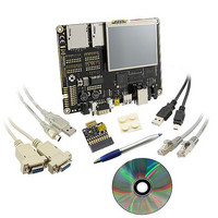
BMSKTOPASA900(DCE) Toshiba, BMSKTOPASA900(DCE) Datasheet - Page 530

BMSKTOPASA900(DCE)
Manufacturer Part Number
BMSKTOPASA900(DCE)
Description
KIT STARTER TMPA900 USB JTAG
Manufacturer
Toshiba
Series
TOPASr
Type
MCUr
Specifications of BMSKTOPASA900(DCE)
Contents
Evaluation Board, Cable(s), Software and Documentation
For Use With/related Products
TMPA900CMXBG
Lead Free Status / RoHS Status
Lead free / RoHS Compliant
- Current page: 530 of 959
- Download datasheet (5Mb)
22. UDC2 (UDC2 register) (0x0200 to 0x03FC)
(0xF440_0000) + 0x200-0x3FC. AHB data bus of UDC2AB has 32 bits, of which bits 15-0
correspond with the UDC2 data bus. Bits 31-16 are reserved bits and read-only (read value: 0).
Make a WORD (32-bit) access for both write and read. (However, a BYTE (8-bit) access may be
made for Write accesses to the EPx_FIFO register. Details will be discussed later.)
UDC2). Be sure to begin subsequent accesses after the previous UDC2 register access is
completed, using the int_udc2_reg_rd interrupt. (You can also use the udc2rdreq bit of UDC2
Read Request register to confirm the access status when reading.)
• Write access
• Read access
• EPx_FIFO register
• Reserved registers in UDC2
• Accesses when UDC2 is suspended
The internal register of UDC2 (16 bits) can be accessed by making an access to the
It will take some time to complete an access for both write and read (accessing period to
address.
Read Value registers.
data from the UDC2 Read Value register for reading. You cannot read the data directly
from the address shown in the address map.
required in UDC2 PVCI I/F. In such a case, make a BYTE access to the lower 1 byte for
UDC2AB.
Read Request register as usual and read the data from UDC2 Read Value register. In that
case, the access to UDC2 Read Value register can be either by WORD or BYTE.
and to “Reserved” registers. (In case those registers are accessed, the access from UDC2AB
to UDC2 itself will take place. It will be a Dummy write to UDC2 in case of write accesses.
In case of read accesses, the read data from UDC2 (udc2_rdata) will be an indefinite value
and the indefinite value will be set to the UDC2 Read Value register.)
the clock (= CLK_U) supply from PHY is stopped. Make no register accesses to UDC2 in
such cases. If the UDC2 register is accessed when the phy_suspend bit of Power Detect
Control register is set to 1, an AHB error will be returned.
When making a write access to the UDC2 register, write it directly in the relevant
When making a read access to the UDC2 register, use UDC2 Read Request and UDC2
First, you set the address to access to the UDC2 Read Request register and then read the
When making a write access to the EPx_FIFO register, a lower 1-byte access may be
If a lower 1-byte access is required when making a read access, make an access via UDC2
Do not make any access to registers of endpoints not supported by UDC2 to be connected
When UDC2 is in the suspended status, register accesses to UDC2 become unavailable if
TENTATIVE
TMPA900CM- 529
TMPA900CM
2009-10-14
Related parts for BMSKTOPASA900(DCE)
Image
Part Number
Description
Manufacturer
Datasheet
Request
R
Part Number:
Description:
Toshiba Semiconductor [TOSHIBA IGBT Module Silicon N Channel IGBT]
Manufacturer:
TOSHIBA Semiconductor CORPORATION
Datasheet:
Part Number:
Description:
TOSHIBA GTR MODULE SILICON NPN TRIPLE DIFFUSED TYPE
Manufacturer:
TOSHIBA Semiconductor CORPORATION
Datasheet:
Part Number:
Description:
TOSHIBA GTR Module Silicon N Channel IGBT
Manufacturer:
TOSHIBA Semiconductor CORPORATION
Datasheet:
Part Number:
Description:
TOSHIBA Intelligent Power Module Silicon N Channel IGBT
Manufacturer:
TOSHIBA Semiconductor CORPORATION
Datasheet:
Part Number:
Description:
TOSHIBA INTELLIGENT POWER MODULE SILICON N CHANNEL LGBT
Manufacturer:
TOSHIBA Semiconductor CORPORATION
Datasheet:
Part Number:
Description:
TOSHIBA IGBT Module Silicon N Channel IGBT
Manufacturer:
TOSHIBA Semiconductor CORPORATION
Datasheet:
Part Number:
Description:
TOSHIBA GTR MODULE SILICON N−CHANNEL IGBT
Manufacturer:
TOSHIBA Semiconductor CORPORATION
Datasheet:
Part Number:
Description:
TOSHIBA Intelligent Power Module Silicon N Channel IGBT
Manufacturer:
TOSHIBA Semiconductor CORPORATION
Datasheet:
Part Number:
Description:
TOSHIBA GTR Module Silicon N Channel IGBT
Manufacturer:
TOSHIBA Semiconductor CORPORATION
Datasheet:
Part Number:
Description:
TOSHIBA INTELLIGENT POWER MODULE
Manufacturer:
TOSHIBA Semiconductor CORPORATION
Datasheet:
Part Number:
Description:
TOSHIBA Intelligent Power Module Silicon N Channel IGBT
Manufacturer:
TOSHIBA Semiconductor CORPORATION
Datasheet:
Part Number:
Description:
TOSHIBA Intelligent Power Module Silicon N Channel IGBT
Manufacturer:
TOSHIBA Semiconductor CORPORATION
Datasheet:
Part Number:
Description:
TOSHIBA IGBT Module Silicon N Channel IGBT
Manufacturer:
TOSHIBA Semiconductor CORPORATION
Datasheet:
Part Number:
Description:
TOSHIBA Intelligent Power Module Silicon N Channel IGBT
Manufacturer:
TOSHIBA Semiconductor CORPORATION
Datasheet:
Part Number:
Description:
Toshiba Semiconductor [SILICON N CHANNEL 1GBT]
Manufacturer:
TOSHIBA Semiconductor CORPORATION
Datasheet:


