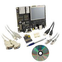
BMSKTOPASA900(DCE) Toshiba, BMSKTOPASA900(DCE) Datasheet - Page 38

BMSKTOPASA900(DCE)
Manufacturer Part Number
BMSKTOPASA900(DCE)
Description
KIT STARTER TMPA900 USB JTAG
Manufacturer
Toshiba
Series
TOPASr
Type
MCUr
Specifications of BMSKTOPASA900(DCE)
Contents
Evaluation Board, Cable(s), Software and Documentation
For Use With/related Products
TMPA900CMXBG
Lead Free Status / RoHS Status
Lead free / RoHS Compliant
- Current page: 38 of 959
- Download datasheet (5Mb)
3.2.6
3.2.7
TMS and TDI are sampled on the rising edge of
Data is scanned in serially.
TCK.
115
3
TCK
cells connected to the input and output pads on the TMPA900CM.
boundary scan register is shifted out on the TDO output.
TCK. These pins control a test by communicating the serial test data and instructions.
register, bypass register or boundary scan register) on the TDI pin, or it is scanned out from
one of these three registers on the TDO pin.
The TCK input is a special test clock that allows serial JTAG data to be shifted
synchronously, independent of any chip-specific or system clocks.
signal. Data on the TDO pin changes on the falling edge of the TCK clock signal.
Boundary Scan Register
Test Access Port (TAP)
processor except some analog outputs and control signals. The pins of the TMPA900CM
allow any pattern to be driven by scanning the data into the boundary scan register in the
Shift-DR state. Incoming data to the processor is examined by enabling the boundary scan
register and shifting the data when the BSR is in the Capture-DR state.
Instruction register
The boundary scan register provides all the inputs and outputs of the TMPA900CM
The boundary scan register is a single, 231-bit-wide, shift register-based path containing
The TDI input is loaded to the LSB of the boundary scan register. The MSB of the
The Test Access Port (TAP) consists of the five signal pins: TRSTn, TDI, TDO, TMS and
As Figure 3.2.5 shows, data is serially scanned into one of the three registers (instruction
The TMS input controls the state transitions of the main TAP controller state machine.
Data on the TDI and TMS pins are sampled on the rising edge of the TCK input clock
Bypass register
Boundary scan
register
0
0
0
Figure 3.2.5 JTAG Test Access Port
TENTATIVE
TMPA900CM- 37
TMS pin
TDI pin
3
115
Instruction register
TDO is sampled on the falling edge of TCK.
Bypass register
Boundary scan
register
0
Data is scanned out serially.
0
0
TMPA900CM
2009-10-14
TDO pin
Related parts for BMSKTOPASA900(DCE)
Image
Part Number
Description
Manufacturer
Datasheet
Request
R
Part Number:
Description:
Toshiba Semiconductor [TOSHIBA IGBT Module Silicon N Channel IGBT]
Manufacturer:
TOSHIBA Semiconductor CORPORATION
Datasheet:
Part Number:
Description:
TOSHIBA GTR MODULE SILICON NPN TRIPLE DIFFUSED TYPE
Manufacturer:
TOSHIBA Semiconductor CORPORATION
Datasheet:
Part Number:
Description:
TOSHIBA GTR Module Silicon N Channel IGBT
Manufacturer:
TOSHIBA Semiconductor CORPORATION
Datasheet:
Part Number:
Description:
TOSHIBA Intelligent Power Module Silicon N Channel IGBT
Manufacturer:
TOSHIBA Semiconductor CORPORATION
Datasheet:
Part Number:
Description:
TOSHIBA INTELLIGENT POWER MODULE SILICON N CHANNEL LGBT
Manufacturer:
TOSHIBA Semiconductor CORPORATION
Datasheet:
Part Number:
Description:
TOSHIBA IGBT Module Silicon N Channel IGBT
Manufacturer:
TOSHIBA Semiconductor CORPORATION
Datasheet:
Part Number:
Description:
TOSHIBA GTR MODULE SILICON N−CHANNEL IGBT
Manufacturer:
TOSHIBA Semiconductor CORPORATION
Datasheet:
Part Number:
Description:
TOSHIBA Intelligent Power Module Silicon N Channel IGBT
Manufacturer:
TOSHIBA Semiconductor CORPORATION
Datasheet:
Part Number:
Description:
TOSHIBA GTR Module Silicon N Channel IGBT
Manufacturer:
TOSHIBA Semiconductor CORPORATION
Datasheet:
Part Number:
Description:
TOSHIBA INTELLIGENT POWER MODULE
Manufacturer:
TOSHIBA Semiconductor CORPORATION
Datasheet:
Part Number:
Description:
TOSHIBA Intelligent Power Module Silicon N Channel IGBT
Manufacturer:
TOSHIBA Semiconductor CORPORATION
Datasheet:
Part Number:
Description:
TOSHIBA Intelligent Power Module Silicon N Channel IGBT
Manufacturer:
TOSHIBA Semiconductor CORPORATION
Datasheet:
Part Number:
Description:
TOSHIBA IGBT Module Silicon N Channel IGBT
Manufacturer:
TOSHIBA Semiconductor CORPORATION
Datasheet:
Part Number:
Description:
TOSHIBA Intelligent Power Module Silicon N Channel IGBT
Manufacturer:
TOSHIBA Semiconductor CORPORATION
Datasheet:
Part Number:
Description:
Toshiba Semiconductor [SILICON N CHANNEL 1GBT]
Manufacturer:
TOSHIBA Semiconductor CORPORATION
Datasheet:


