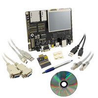
BMSKTOPASA900(DCE) Toshiba, BMSKTOPASA900(DCE) Datasheet - Page 449

BMSKTOPASA900(DCE)
Manufacturer Part Number
BMSKTOPASA900(DCE)
Description
KIT STARTER TMPA900 USB JTAG
Manufacturer
Toshiba
Series
TOPASr
Type
MCUr
Specifications of BMSKTOPASA900(DCE)
Contents
Evaluation Board, Cable(s), Software and Documentation
For Use With/related Products
TMPA900CMXBG
Lead Free Status / RoHS Status
Lead free / RoHS Compliant
- Current page: 449 of 959
- Download datasheet (5Mb)
I2C0SR<PIN>
I2C0CL
I2CINT0 interrupt request signal
3.14.6.7 Interrupt Service Request and Cancel
I2C0CR1<ACK> have been transferred, an I2CINT0 interrupt request is generated.
conditions in addition to the above condition:
I2C0SR<PIN> is 0, I2C0CL is pulled low.
I2C0CR2<PIN> can be set to 1 by writing 1 whereas it cannot be cleared to 0 by writing 0.
•
•
•
In master mode, after the number of bits specified by I2C0CR1<BC> and
In slave mode, an I2CINT0 interrupt request is also generated by the following
When an I2CINT0 interrupt request is generated, I2C0SR<PIN> is cleared to 0. While
Writing data into I2C0DBR sets I2C0SR<PIN> to 1.
It takes the t
1
When I2C0CR1<NOACK> is 0, after the acknowledge signal is output to indicate
that the received slave address has matched the slave address set in I2C0AR<SA>
When I2C0CR1<NOACK> is 0, after the acknowledge signal is output to indicate
that a general call has been received.
When data transfer is completed after a matched slave address or a general call is
received.
2
LOW
Figure 3.14.17 I2C0SR<PIN> and I2C0CL
3
period for I2C0CL to be released after I2C0SR<PIN> is set to 1.
TENTATIVE
TMPA900CM- 448
7
8
9
I2C0CL is pulled
low while
I2C0SR<PIN> = 0.
t
LOW
or a write to I2C0DBR
I2C0CR2<PIN> = 1
1
TMPA900CM
2009-10-14
Related parts for BMSKTOPASA900(DCE)
Image
Part Number
Description
Manufacturer
Datasheet
Request
R
Part Number:
Description:
Toshiba Semiconductor [TOSHIBA IGBT Module Silicon N Channel IGBT]
Manufacturer:
TOSHIBA Semiconductor CORPORATION
Datasheet:
Part Number:
Description:
TOSHIBA GTR MODULE SILICON NPN TRIPLE DIFFUSED TYPE
Manufacturer:
TOSHIBA Semiconductor CORPORATION
Datasheet:
Part Number:
Description:
TOSHIBA GTR Module Silicon N Channel IGBT
Manufacturer:
TOSHIBA Semiconductor CORPORATION
Datasheet:
Part Number:
Description:
TOSHIBA Intelligent Power Module Silicon N Channel IGBT
Manufacturer:
TOSHIBA Semiconductor CORPORATION
Datasheet:
Part Number:
Description:
TOSHIBA INTELLIGENT POWER MODULE SILICON N CHANNEL LGBT
Manufacturer:
TOSHIBA Semiconductor CORPORATION
Datasheet:
Part Number:
Description:
TOSHIBA IGBT Module Silicon N Channel IGBT
Manufacturer:
TOSHIBA Semiconductor CORPORATION
Datasheet:
Part Number:
Description:
TOSHIBA GTR MODULE SILICON N−CHANNEL IGBT
Manufacturer:
TOSHIBA Semiconductor CORPORATION
Datasheet:
Part Number:
Description:
TOSHIBA Intelligent Power Module Silicon N Channel IGBT
Manufacturer:
TOSHIBA Semiconductor CORPORATION
Datasheet:
Part Number:
Description:
TOSHIBA GTR Module Silicon N Channel IGBT
Manufacturer:
TOSHIBA Semiconductor CORPORATION
Datasheet:
Part Number:
Description:
TOSHIBA INTELLIGENT POWER MODULE
Manufacturer:
TOSHIBA Semiconductor CORPORATION
Datasheet:
Part Number:
Description:
TOSHIBA Intelligent Power Module Silicon N Channel IGBT
Manufacturer:
TOSHIBA Semiconductor CORPORATION
Datasheet:
Part Number:
Description:
TOSHIBA Intelligent Power Module Silicon N Channel IGBT
Manufacturer:
TOSHIBA Semiconductor CORPORATION
Datasheet:
Part Number:
Description:
TOSHIBA IGBT Module Silicon N Channel IGBT
Manufacturer:
TOSHIBA Semiconductor CORPORATION
Datasheet:
Part Number:
Description:
TOSHIBA Intelligent Power Module Silicon N Channel IGBT
Manufacturer:
TOSHIBA Semiconductor CORPORATION
Datasheet:
Part Number:
Description:
Toshiba Semiconductor [SILICON N CHANNEL 1GBT]
Manufacturer:
TOSHIBA Semiconductor CORPORATION
Datasheet:


