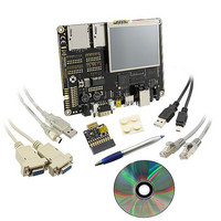
BMSKTOPASA900(DCE) Toshiba, BMSKTOPASA900(DCE) Datasheet - Page 324

BMSKTOPASA900(DCE)
Manufacturer Part Number
BMSKTOPASA900(DCE)
Description
KIT STARTER TMPA900 USB JTAG
Manufacturer
Toshiba
Series
TOPASr
Type
MCUr
Specifications of BMSKTOPASA900(DCE)
Contents
Evaluation Board, Cable(s), Software and Documentation
For Use With/related Products
TMPA900CMXBG
Lead Free Status / RoHS Status
Lead free / RoHS Compliant
- Current page: 324 of 959
- Download datasheet (5Mb)
3. NDFMCR2 (NAND-Flash Control Register 2)
[31:15]
[14:12]
[11]
[10:8]
[7]
[6:4]
[3]
[2:0]
[Description]
Bit
a. <SPLW>, <SPHW>, <SPLR>, <SPHR>
0y111 are prohibited.
These are registers to set the Low and High pulse width of the NDREn and NDWEn pins.
The pulse width is given by the set value × the period of HCLK. Setting 0y000, 0y110 and
Symbol
−
SPLW
−
SPHW
−
SPLR
−
SPHR
Bit
−
R/W
−
R/W
−
R/W
−
R/W
Type
Undefined
0y000
Undefined
0y000
Undefined
0y000
Undefined
0y000
Reset
Value
TENTATIVE
TMPA900CM- 323
Read undefined. Write as zero.
NDWEn Low pulse width setting
Read undefined. Write as zero.
NDWEn High pulse width setting
Read undefined. Write as zero.
NDREn Low pulse width setting
Read undefined. Write as zero.
NDREn High pulse width setting
0y000: Reserved
0y001: 1 cycle of HCLK
0y010: 2 cycles of HCLK
0y011: 3 cycles of HCLK
0y100: 4 cycles of HCLK
0y101: 5 cycles of HCLK
0y110-0y111: Reserved
0y000: Reserved
0y001: 1 cycle of HCLK
0y010: 2 cycles of HCLK
0y011: 3 cycles of HCLK
0y00: 4 cycles of HCLK
0y101: 5 cycles of HCLK
0y110-0y111: Reserved
0y000: Reserved
0y001: 1 cycle of HCLK
0y010: 2 cycles of HCLK
0y011: 3 cycles of HCLK
0y100: 4 cycles of HCLK
0y101: 5 cycles of HCLK
0y110-0y111: Reserved
0y000: Reserved
0y001: 1 cycle of HCLK
0y010: 2 cycles of HCLK
0y011: 3 cycles of HCLK
0y100: 4 cycles of HCLK
0y101: 5 cycles of HCLK
0y110-0y111: Reserved
Description
Address = (0xf201_0000) + (0x0008)
TMPA900CM
2009-10-14
Related parts for BMSKTOPASA900(DCE)
Image
Part Number
Description
Manufacturer
Datasheet
Request
R
Part Number:
Description:
Toshiba Semiconductor [TOSHIBA IGBT Module Silicon N Channel IGBT]
Manufacturer:
TOSHIBA Semiconductor CORPORATION
Datasheet:
Part Number:
Description:
TOSHIBA GTR MODULE SILICON NPN TRIPLE DIFFUSED TYPE
Manufacturer:
TOSHIBA Semiconductor CORPORATION
Datasheet:
Part Number:
Description:
TOSHIBA GTR Module Silicon N Channel IGBT
Manufacturer:
TOSHIBA Semiconductor CORPORATION
Datasheet:
Part Number:
Description:
TOSHIBA Intelligent Power Module Silicon N Channel IGBT
Manufacturer:
TOSHIBA Semiconductor CORPORATION
Datasheet:
Part Number:
Description:
TOSHIBA INTELLIGENT POWER MODULE SILICON N CHANNEL LGBT
Manufacturer:
TOSHIBA Semiconductor CORPORATION
Datasheet:
Part Number:
Description:
TOSHIBA IGBT Module Silicon N Channel IGBT
Manufacturer:
TOSHIBA Semiconductor CORPORATION
Datasheet:
Part Number:
Description:
TOSHIBA GTR MODULE SILICON N−CHANNEL IGBT
Manufacturer:
TOSHIBA Semiconductor CORPORATION
Datasheet:
Part Number:
Description:
TOSHIBA Intelligent Power Module Silicon N Channel IGBT
Manufacturer:
TOSHIBA Semiconductor CORPORATION
Datasheet:
Part Number:
Description:
TOSHIBA GTR Module Silicon N Channel IGBT
Manufacturer:
TOSHIBA Semiconductor CORPORATION
Datasheet:
Part Number:
Description:
TOSHIBA INTELLIGENT POWER MODULE
Manufacturer:
TOSHIBA Semiconductor CORPORATION
Datasheet:
Part Number:
Description:
TOSHIBA Intelligent Power Module Silicon N Channel IGBT
Manufacturer:
TOSHIBA Semiconductor CORPORATION
Datasheet:
Part Number:
Description:
TOSHIBA Intelligent Power Module Silicon N Channel IGBT
Manufacturer:
TOSHIBA Semiconductor CORPORATION
Datasheet:
Part Number:
Description:
TOSHIBA IGBT Module Silicon N Channel IGBT
Manufacturer:
TOSHIBA Semiconductor CORPORATION
Datasheet:
Part Number:
Description:
TOSHIBA Intelligent Power Module Silicon N Channel IGBT
Manufacturer:
TOSHIBA Semiconductor CORPORATION
Datasheet:
Part Number:
Description:
Toshiba Semiconductor [SILICON N CHANNEL 1GBT]
Manufacturer:
TOSHIBA Semiconductor CORPORATION
Datasheet:


