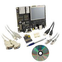
BMSKTOPASA900(DCE) Toshiba, BMSKTOPASA900(DCE) Datasheet - Page 761

BMSKTOPASA900(DCE)
Manufacturer Part Number
BMSKTOPASA900(DCE)
Description
KIT STARTER TMPA900 USB JTAG
Manufacturer
Toshiba
Series
TOPASr
Type
MCUr
Specifications of BMSKTOPASA900(DCE)
Contents
Evaluation Board, Cable(s), Software and Documentation
For Use With/related Products
TMPA900CMXBG
Lead Free Status / RoHS Status
Lead free / RoHS Compliant
- Current page: 761 of 959
- Download datasheet (5Mb)
CMSSCDMA
Input Data
CMSYD
CMSUD
CMSVD
・Data Input from Internal Registers
Note : Dummy data is added only when the window of the FIFO buffer read register is configured to read 4 bytes of data at a
Format
time (CMCCR<CSFOW> = 0). Please note that dummy data is not added if CMCCR<CSFOW> = 1 (a byte of data
reading). Refer to3.22.2.4(4) “Formats of RGB Storage from FIFO buffer into the CMSFPT register” for details.
(2) When the color space conversion circuit is used by writing YUV data in internal
this happens, reset the FIFO pointer by using CMSCR<CFPCLR> and then write new
YUV data.
FIFO Output Format
sequentially. When used by the CPU, INTCMSF is also generated when 32 bytes or
more of data are stored in the FIFO or when 48 bytes or more of data are stored in the
FIFO, as in the case of connecting a CMOS image sensor. For details, see the table
below.
registers without connecting a CMOS image sensor (CMSCV<CCVM1:0> = 0y10 or
0y11)
Without Dummy
Without Dummy
The RGB data generated by the color space conversion circuit is stored in the FIFO
Reading the FIFO while valid data is not stored in it corrupts the FIFO pointer. If
With Dummy
With Dummy
*Note
*Note
TENTATIVE
TMPA900CM- 760
FIFO interrupt
Water_Mark
32bytes
48bytes
32bytes
48bytes
Output Data
RGB5:6:5
RGB8:8:8
RGB5:6:5
RGB8:8:8
Format
CRGBM
0
1
0
1
CMSCV Register
Configuration
CCVM1
TMPA900CM
1
1
1
1
2009-10-14
CCVM0
0
0
1
1
Related parts for BMSKTOPASA900(DCE)
Image
Part Number
Description
Manufacturer
Datasheet
Request
R
Part Number:
Description:
Toshiba Semiconductor [TOSHIBA IGBT Module Silicon N Channel IGBT]
Manufacturer:
TOSHIBA Semiconductor CORPORATION
Datasheet:
Part Number:
Description:
TOSHIBA GTR MODULE SILICON NPN TRIPLE DIFFUSED TYPE
Manufacturer:
TOSHIBA Semiconductor CORPORATION
Datasheet:
Part Number:
Description:
TOSHIBA GTR Module Silicon N Channel IGBT
Manufacturer:
TOSHIBA Semiconductor CORPORATION
Datasheet:
Part Number:
Description:
TOSHIBA Intelligent Power Module Silicon N Channel IGBT
Manufacturer:
TOSHIBA Semiconductor CORPORATION
Datasheet:
Part Number:
Description:
TOSHIBA INTELLIGENT POWER MODULE SILICON N CHANNEL LGBT
Manufacturer:
TOSHIBA Semiconductor CORPORATION
Datasheet:
Part Number:
Description:
TOSHIBA IGBT Module Silicon N Channel IGBT
Manufacturer:
TOSHIBA Semiconductor CORPORATION
Datasheet:
Part Number:
Description:
TOSHIBA GTR MODULE SILICON N−CHANNEL IGBT
Manufacturer:
TOSHIBA Semiconductor CORPORATION
Datasheet:
Part Number:
Description:
TOSHIBA Intelligent Power Module Silicon N Channel IGBT
Manufacturer:
TOSHIBA Semiconductor CORPORATION
Datasheet:
Part Number:
Description:
TOSHIBA GTR Module Silicon N Channel IGBT
Manufacturer:
TOSHIBA Semiconductor CORPORATION
Datasheet:
Part Number:
Description:
TOSHIBA INTELLIGENT POWER MODULE
Manufacturer:
TOSHIBA Semiconductor CORPORATION
Datasheet:
Part Number:
Description:
TOSHIBA Intelligent Power Module Silicon N Channel IGBT
Manufacturer:
TOSHIBA Semiconductor CORPORATION
Datasheet:
Part Number:
Description:
TOSHIBA Intelligent Power Module Silicon N Channel IGBT
Manufacturer:
TOSHIBA Semiconductor CORPORATION
Datasheet:
Part Number:
Description:
TOSHIBA IGBT Module Silicon N Channel IGBT
Manufacturer:
TOSHIBA Semiconductor CORPORATION
Datasheet:
Part Number:
Description:
TOSHIBA Intelligent Power Module Silicon N Channel IGBT
Manufacturer:
TOSHIBA Semiconductor CORPORATION
Datasheet:
Part Number:
Description:
Toshiba Semiconductor [SILICON N CHANNEL 1GBT]
Manufacturer:
TOSHIBA Semiconductor CORPORATION
Datasheet:


