M30845FJGP#U3 Renesas Electronics America, M30845FJGP#U3 Datasheet - Page 141
M30845FJGP#U3
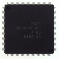
Manufacturer Part Number
M30845FJGP#U3
Description
IC M32C MCU FLASH 512K 144LQFP
Manufacturer
Renesas Electronics America
Series
M16C™ M32C/80r
Specifications of M30845FJGP#U3
Core Processor
M32C/80
Core Size
16/32-Bit
Speed
32MHz
Connectivity
CAN, I²C, IEBus, SIO, UART/USART
Peripherals
DMA, PWM, WDT
Number Of I /o
121
Program Memory Size
512KB (512K x 8)
Program Memory Type
FLASH
Ram Size
24K x 8
Voltage - Supply (vcc/vdd)
3 V ~ 5.5 V
Data Converters
A/D 34x10b, D/A 2x8b
Oscillator Type
Internal
Operating Temperature
-40°C ~ 85°C
Package / Case
144-LQFP
Lead Free Status / RoHS Status
Lead free / RoHS Compliant
Eeprom Size
-
Available stocks
Company
Part Number
Manufacturer
Quantity
Price


R
R
M
e
E
3
. v
J
2
0
C
11.6.3 Interrupt Sequence
1
9
0 .
8 /
B
The interrupt sequence is performed between an interrupt request acknowledgment and interrupt routine
execution.
When an interrupt request is generated while an instruction is executed, the CPU determines its interrupt
priority level after the instruction is completed. The CPU starts the interrupt sequence from the following
cycle. However, in regards to the SCMPU, SIN, SMOVB, SMOVF, SMOVU, SSTR, SOUT or RMPA
instruction, if an interrupt request is generated while executing the instruction, the microcomputer sus-
pends the instruction to start the interrupt sequence.
The interrupt sequence is performed as follows:
(1) The CPU obtains interrupt information (interrupt number and interrupt request level) by reading
(2) The FLG register, prior to an interrupt sequence, is saved to a temporary register
(3) Each bit in the FLG register is set as follows:
(4) A temporary register within the CPU is saved to the stack; or to the SVF register for the high-speed
(5) PC is saved to the stack; or to the SVP register for the high-speed interrupt.
(6) The interrupt priority level of the acknowledged interrupt is set in IPL .
(7) A relocatable vector corresponding to the acknowledged interrupt is stored into PC.
After the interrupt sequence is completed, an instruction is executed from the starting address of the
interrupt routine.
NOTES:
0
1
4
1. Temporary register cannot be modified by users.
0
3
G
J
address 000000
the interrupt information is set to "0" (interrupt requested).
interrupt.
6
u
o r
0 -
. l
• The I flag is set to "0" (interrupt disabled)
• The D flag is set to "0" (single-step disabled)
• The U flag is set to "0" (ISP selected)
u
0
1
, 7
0
p
1
(
2
M
0
0
3
5
2
C
8 /
Page 118
, 4
16
M
(address 000002
3
2
C
f o
8 /
4
4
) T
9
5
16
for the high-speed interrupt). Then, the IR bit applicable to
(1)
within the CPU.
11. Interrupts
Related parts for M30845FJGP#U3
Image
Part Number
Description
Manufacturer
Datasheet
Request
R

Part Number:
Description:
KIT STARTER FOR M16C/29
Manufacturer:
Renesas Electronics America
Datasheet:

Part Number:
Description:
KIT STARTER FOR R8C/2D
Manufacturer:
Renesas Electronics America
Datasheet:

Part Number:
Description:
R0K33062P STARTER KIT
Manufacturer:
Renesas Electronics America
Datasheet:

Part Number:
Description:
KIT STARTER FOR R8C/23 E8A
Manufacturer:
Renesas Electronics America
Datasheet:

Part Number:
Description:
KIT STARTER FOR R8C/25
Manufacturer:
Renesas Electronics America
Datasheet:

Part Number:
Description:
KIT STARTER H8S2456 SHARPE DSPLY
Manufacturer:
Renesas Electronics America
Datasheet:

Part Number:
Description:
KIT STARTER FOR R8C38C
Manufacturer:
Renesas Electronics America
Datasheet:

Part Number:
Description:
KIT STARTER FOR R8C35C
Manufacturer:
Renesas Electronics America
Datasheet:

Part Number:
Description:
KIT STARTER FOR R8CL3AC+LCD APPS
Manufacturer:
Renesas Electronics America
Datasheet:
Part Number:
Description:
KIT STARTER FOR RX610
Manufacturer:
Renesas Electronics America
Datasheet:

Part Number:
Description:
KIT STARTER FOR R32C/118
Manufacturer:
Renesas Electronics America
Datasheet:

Part Number:
Description:
KIT DEV RSK-R8C/26-29
Manufacturer:
Renesas Electronics America
Datasheet:

Part Number:
Description:
KIT STARTER FOR SH7124
Manufacturer:
Renesas Electronics America
Datasheet:

Part Number:
Description:
KIT STARTER FOR H8SX/1622
Manufacturer:
Renesas Electronics America
Datasheet:

Part Number:
Description:
KIT DEV FOR SH7203
Manufacturer:
Renesas Electronics America
Datasheet: