M30845FJGP#U3 Renesas Electronics America, M30845FJGP#U3 Datasheet - Page 7
M30845FJGP#U3
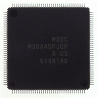
Manufacturer Part Number
M30845FJGP#U3
Description
IC M32C MCU FLASH 512K 144LQFP
Manufacturer
Renesas Electronics America
Series
M16C™ M32C/80r
Specifications of M30845FJGP#U3
Core Processor
M32C/80
Core Size
16/32-Bit
Speed
32MHz
Connectivity
CAN, I²C, IEBus, SIO, UART/USART
Peripherals
DMA, PWM, WDT
Number Of I /o
121
Program Memory Size
512KB (512K x 8)
Program Memory Type
FLASH
Ram Size
24K x 8
Voltage - Supply (vcc/vdd)
3 V ~ 5.5 V
Data Converters
A/D 34x10b, D/A 2x8b
Oscillator Type
Internal
Operating Temperature
-40°C ~ 85°C
Package / Case
144-LQFP
Lead Free Status / RoHS Status
Lead free / RoHS Compliant
Eeprom Size
-
Available stocks
Company
Part Number
Manufacturer
Quantity
Price


7. Processor Mode ______________________________ 55
8. Bus_________________________________________ 60
9. Clock Generation Circuit _______________________ 81
A-2
7.1 Types of Processor Mode ........................................................................................ 55
7.2 Setting of Processor Mode ...................................................................................... 56
8.1 Bus Settings ............................................................................................................. 60
8.2 Bus Control ............................................................................................................... 63
8.3 Page Mode Control Function .................................................................................. 77
9.1 Types of the Clock Generation Circuit ................................................................... 81
9.2 CPU Clock and BCLK .............................................................................................. 95
9.3 Peripheral Function Clock ....................................................................................... 95
9.4 Clock Output Function ............................................................................................ 96
9.5 Power Consumption Control .................................................................................. 97
9.6 System Clock Protect Function ............................................................................ 105
8.1.1 Selecting External Address Bus ...................................................................... 61
8.1.2 Selecting External Data Bus ............................................................................ 61
8.1.3 Selecting Separate/Multiplexed Bus ............................................................... 61
8.2.1 Address Bus and Data Bus .............................................................................. 63
8.2.2 Chip-Select Signal ............................................................................................ 63
8.2.3 Read and Write Signals .................................................................................... 65
8.2.4 Bus Timing ........................................................................................................ 66
8.2.5 ALE Signal ......................................................................................................... 74
8.2.6 RDY Signal ......................................................................................................... 74
8.2.7 HOLD Signal ...................................................................................................... 76
8.2.8 External Bus Status when Accessing Internal Space ................................... 76
8.2.9 BCLK Output ..................................................................................................... 76
9.1.1 Main Clock ......................................................................................................... 90
9.1.2 Sub Clock .......................................................................................................... 91
9.1.3 On-Chip Oscillator Clock ................................................................................. 92
9.1.4 PLL Clock .......................................................................................................... 94
9.3.1 f
9.3.2 f
9.3.3 fC
9.3.4 f
9.5.1 Normal Operating Mode ................................................................................... 97
9.5.2 Wait Mode .......................................................................................................... 98
9.5.3 Stop Mode ........................................................................................................ 100
_______
_________
1
AD ....................................................................................................................................................
CAN ..................................................................................................................................................
, f
32 ..................................................................................................................................................
8
, f
32
and f
2n .........................................................................................................................
95
95
96
96
Related parts for M30845FJGP#U3
Image
Part Number
Description
Manufacturer
Datasheet
Request
R

Part Number:
Description:
KIT STARTER FOR M16C/29
Manufacturer:
Renesas Electronics America
Datasheet:

Part Number:
Description:
KIT STARTER FOR R8C/2D
Manufacturer:
Renesas Electronics America
Datasheet:

Part Number:
Description:
R0K33062P STARTER KIT
Manufacturer:
Renesas Electronics America
Datasheet:

Part Number:
Description:
KIT STARTER FOR R8C/23 E8A
Manufacturer:
Renesas Electronics America
Datasheet:

Part Number:
Description:
KIT STARTER FOR R8C/25
Manufacturer:
Renesas Electronics America
Datasheet:

Part Number:
Description:
KIT STARTER H8S2456 SHARPE DSPLY
Manufacturer:
Renesas Electronics America
Datasheet:

Part Number:
Description:
KIT STARTER FOR R8C38C
Manufacturer:
Renesas Electronics America
Datasheet:

Part Number:
Description:
KIT STARTER FOR R8C35C
Manufacturer:
Renesas Electronics America
Datasheet:

Part Number:
Description:
KIT STARTER FOR R8CL3AC+LCD APPS
Manufacturer:
Renesas Electronics America
Datasheet:
Part Number:
Description:
KIT STARTER FOR RX610
Manufacturer:
Renesas Electronics America
Datasheet:

Part Number:
Description:
KIT STARTER FOR R32C/118
Manufacturer:
Renesas Electronics America
Datasheet:

Part Number:
Description:
KIT DEV RSK-R8C/26-29
Manufacturer:
Renesas Electronics America
Datasheet:

Part Number:
Description:
KIT STARTER FOR SH7124
Manufacturer:
Renesas Electronics America
Datasheet:

Part Number:
Description:
KIT STARTER FOR H8SX/1622
Manufacturer:
Renesas Electronics America
Datasheet:

Part Number:
Description:
KIT DEV FOR SH7203
Manufacturer:
Renesas Electronics America
Datasheet: