M30845FJGP#U3 Renesas Electronics America, M30845FJGP#U3 Datasheet - Page 340
M30845FJGP#U3
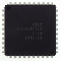
Manufacturer Part Number
M30845FJGP#U3
Description
IC M32C MCU FLASH 512K 144LQFP
Manufacturer
Renesas Electronics America
Series
M16C™ M32C/80r
Specifications of M30845FJGP#U3
Core Processor
M32C/80
Core Size
16/32-Bit
Speed
32MHz
Connectivity
CAN, I²C, IEBus, SIO, UART/USART
Peripherals
DMA, PWM, WDT
Number Of I /o
121
Program Memory Size
512KB (512K x 8)
Program Memory Type
FLASH
Ram Size
24K x 8
Voltage - Supply (vcc/vdd)
3 V ~ 5.5 V
Data Converters
A/D 34x10b, D/A 2x8b
Oscillator Type
Internal
Operating Temperature
-40°C ~ 85°C
Package / Case
144-LQFP
Lead Free Status / RoHS Status
Lead free / RoHS Compliant
Eeprom Size
-
Available stocks
Company
Part Number
Manufacturer
Quantity
Price


M
R
R
e
E
3
. v
J
2
Table 22.25 HDLC Processing Mode Specifications (Communication Units 0 and 1)
0
C
22.4.3 HDLC Data Processing Mode (Communication Units 0 and 1)
Input Data Format
Output Data Format
Transfer Clock
I/O Method
Bit Stuffing
Flag Detection
Abort Detection
CRC
Data Processing Start
Condition
1
9
0 .
8 /
B
In HDLC data processing mode, bit stuffing, flag detection, abort detection and CRC calculation are avail-
able for HDLC control. f
generated in the channel 0 or 1, can become the communication unit 1 transfer clock. No pins are used.
To convert data, data to be transmitted is written to the GiTB register (i=0,1) and the data conversion
result is restored after data conversion. If any data are in the GiTO register after data conversion, the
conversion is terminated. If no data is in the GiTO register, bit stuffing processing is executed regardless
of there being no data in the transmit output buffer. A CRC value is calculated every time one bit is
converted. If no data is in the GiRI register, received data conversion is terminated.
Table 22.25 list specifications of the HDLC data processing mode. Tables 22.26 and 22.27 list clock
settings. Table 22.28 lists register settings.
0
1
4
0
3
G
J
6
u
o r
0 -
. l
u
0
1
p
, 7
0
Item
1
(
2
M
0
3
0
2
5
C
8 /
Page 317
, 4
M
3
1
, f
2
8-bit data fixed, bit alignment is optional
8-bit data fixed
See Tables 22.26 and 22.27
• During transmit data processing,
• During received data processing,
During received data processing, "0" following five continuous "1" is deleted.
Write the flag data "7E
nication interrupt (the SRTiR bit in the IIO4IR register)
Write the masked data "01
The CRC1 and CRC0 bits are set to "11
The CRCV bit is set to "1" (set to "FFFF
• During transmit data processing,
• During received data processing,
The following conditions are required to start transmit data processing:
During transmit data processing, "0" following five continuous "1" is inserted.
C
8
The following conditions are required to start receive data processing:
The CRC calculation result is reset when the TE bit in the GiCR register is set to "0"
The CRC calculation result is reset by comparing the flag data "7E
CRC calculation result is stored into the GiTCRC register. The TCRCE bit in the
GiETC register is set to "1" (transmit CRC used).
CRC calculation result is stored into the GiRCRC register. The RCRCE bit in the
GiERC register is set to "1" (receive CRC used).
(transmit disabled).
the result with the value in the GiCMP3 register. The ACRC bit in the GiEMR regis-
ter is set to "1" (CRC reset).
f o
8 /
transferred to the GiTO register.
value set in the GiTB register is converted in HDLC data processing mode and
value set in the GiRI register is converted in HDLC data processing mode and
transferred to the GiRB register. The value in the GiRI register is also transferred to
the GiTB register (received data register).
• The TE bit in the GiCR register is set to "1" (transmit enable)
• Data is written to the GiTB register
• The RE bit in the GiCR register is set to "1" (receive enable)
• Data is written to the GiRI register
or f
4
4
) T
9
2n
5
can become the communication unit 0 transfer clock. f
16
" to the GiCMPj register (j=0 to 3) to use the special commu-
16
" to the GiMSKj register
Specification
22. Intelligent I/O (Communication Function)
2
16
" (X
").
16
+X
12
+X
5
+1).
1
16
, f
" and matching
8
, f
2n
or clock,
Related parts for M30845FJGP#U3
Image
Part Number
Description
Manufacturer
Datasheet
Request
R

Part Number:
Description:
KIT STARTER FOR M16C/29
Manufacturer:
Renesas Electronics America
Datasheet:

Part Number:
Description:
KIT STARTER FOR R8C/2D
Manufacturer:
Renesas Electronics America
Datasheet:

Part Number:
Description:
R0K33062P STARTER KIT
Manufacturer:
Renesas Electronics America
Datasheet:

Part Number:
Description:
KIT STARTER FOR R8C/23 E8A
Manufacturer:
Renesas Electronics America
Datasheet:

Part Number:
Description:
KIT STARTER FOR R8C/25
Manufacturer:
Renesas Electronics America
Datasheet:

Part Number:
Description:
KIT STARTER H8S2456 SHARPE DSPLY
Manufacturer:
Renesas Electronics America
Datasheet:

Part Number:
Description:
KIT STARTER FOR R8C38C
Manufacturer:
Renesas Electronics America
Datasheet:

Part Number:
Description:
KIT STARTER FOR R8C35C
Manufacturer:
Renesas Electronics America
Datasheet:

Part Number:
Description:
KIT STARTER FOR R8CL3AC+LCD APPS
Manufacturer:
Renesas Electronics America
Datasheet:
Part Number:
Description:
KIT STARTER FOR RX610
Manufacturer:
Renesas Electronics America
Datasheet:

Part Number:
Description:
KIT STARTER FOR R32C/118
Manufacturer:
Renesas Electronics America
Datasheet:

Part Number:
Description:
KIT DEV RSK-R8C/26-29
Manufacturer:
Renesas Electronics America
Datasheet:

Part Number:
Description:
KIT STARTER FOR SH7124
Manufacturer:
Renesas Electronics America
Datasheet:

Part Number:
Description:
KIT STARTER FOR H8SX/1622
Manufacturer:
Renesas Electronics America
Datasheet:

Part Number:
Description:
KIT DEV FOR SH7203
Manufacturer:
Renesas Electronics America
Datasheet: