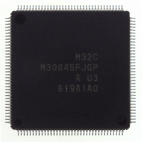
M30845FJGP#U3 Renesas Electronics America, M30845FJGP#U3 Datasheet - Page 262

M30845FJGP#U3
Manufacturer Part Number
M30845FJGP#U3
Description
IC M32C MCU FLASH 512K 144LQFP
Manufacturer
Renesas Electronics America
Series
M16C™ M32C/80r
Specifications of M30845FJGP#U3
Core Processor
M32C/80
Core Size
16/32-Bit
Speed
32MHz
Connectivity
CAN, I²C, IEBus, SIO, UART/USART
Peripherals
DMA, PWM, WDT
Number Of I /o
121
Program Memory Size
512KB (512K x 8)
Program Memory Type
FLASH
Ram Size
24K x 8
Voltage - Supply (vcc/vdd)
3 V ~ 5.5 V
Data Converters
A/D 34x10b, D/A 2x8b
Oscillator Type
Internal
Operating Temperature
-40°C ~ 85°C
Package / Case
144-LQFP
Lead Free Status / RoHS Status
Lead free / RoHS Compliant
Eeprom Size
-
Available stocks
Company
Part Number
Manufacturer
Quantity
Price
- Current page: 262 of 531
- Download datasheet (4Mb)
R
R
M
e
E
3
. v
J
2
Figure 17.28 Bit Function Related Bus Conflict Detection
0
C
1
9
0 .
8 /
B
0
1
4
TxDi
Timer Aj
Transfer Clock
RxDi
TxDi
TxDi
Transfer Clock
TxDi
RxDi
IR bit in
BCNilC register
TE bit in
UiC1 register
Transfer Clock
CLKi
RxDi
0
(1) The ABSCS Bit in the UiSMR Register (Bus conflict and sampling clock selected)
(3) The SSS bit in the UiSMR Register (Transmit start condition selected)
(2) The ACSE Bit in the UiSMR Register (Transmit enable bit is automatically cleared)
3
G
J
6
u
NOTES:
o r
0 -
. l
(i=0 to 4)
1. Data is transmitted on the falling edge of a signal applied to the RxDi pin when the IOPOL bit is set to "0".
2. Data transmission condition must be met before the falling edge of the RxDi pin.
u
0
1
, 7
0
p
Data is transmitted on the rising edge of a signal applied to the RxDi pin when the IOPOL bit is set to "1".
1
(
2
M
0
When the SSS bit is set to "0", data is transmitted after one transfer clock cycle
if data transmission is enabled.
When the SSS bit is set to "1", data is transmitted on the falling edge of the RxDi pin
0
3
5
2
C
8 /
Page 239
, 4
Timer Aj: timer A3 in UART0 or UART3, timer A4 in UART1 or UART4, timer A0 in UART2
transmit enable conditons are met
(Note 2)
M
3
Bus conflict is detected on the rising edge of the transfer clock
when the ABSCS bit is set to "0"
2
C
ST
Trigger signal is applied to the TAj
ST
f o
8 /
4
4
) T
9
5
When ABSCS is set to "1", bus conflict is detected when the timer Aj underflows
(in the one-shot timer mode). An interrupt request is generated.
ST
ST
D
D
0
0
D
D
0
0
D
D
1
1
D
D
1
1
D
D
2
2
D
D
2
2
D
D
3
3
IN
D
D
pin
3
3
D
D
4
4
D
D
4
4
D
D
5
5
D
D
5
5
D
D
6
6
17. Serial I/O (Special Function)
D
D
6
6
D
D
7
7
(1)
D
D
7
7
D
D
8
8
D
D
8
8
SP
SP
SP
SP
Related parts for M30845FJGP#U3
Image
Part Number
Description
Manufacturer
Datasheet
Request
R

Part Number:
Description:
KIT STARTER FOR M16C/29
Manufacturer:
Renesas Electronics America
Datasheet:

Part Number:
Description:
KIT STARTER FOR R8C/2D
Manufacturer:
Renesas Electronics America
Datasheet:

Part Number:
Description:
R0K33062P STARTER KIT
Manufacturer:
Renesas Electronics America
Datasheet:

Part Number:
Description:
KIT STARTER FOR R8C/23 E8A
Manufacturer:
Renesas Electronics America
Datasheet:

Part Number:
Description:
KIT STARTER FOR R8C/25
Manufacturer:
Renesas Electronics America
Datasheet:

Part Number:
Description:
KIT STARTER H8S2456 SHARPE DSPLY
Manufacturer:
Renesas Electronics America
Datasheet:

Part Number:
Description:
KIT STARTER FOR R8C38C
Manufacturer:
Renesas Electronics America
Datasheet:

Part Number:
Description:
KIT STARTER FOR R8C35C
Manufacturer:
Renesas Electronics America
Datasheet:

Part Number:
Description:
KIT STARTER FOR R8CL3AC+LCD APPS
Manufacturer:
Renesas Electronics America
Datasheet:

Part Number:
Description:
KIT STARTER FOR RX610
Manufacturer:
Renesas Electronics America
Datasheet:

Part Number:
Description:
KIT STARTER FOR R32C/118
Manufacturer:
Renesas Electronics America
Datasheet:

Part Number:
Description:
KIT DEV RSK-R8C/26-29
Manufacturer:
Renesas Electronics America
Datasheet:

Part Number:
Description:
KIT STARTER FOR SH7124
Manufacturer:
Renesas Electronics America
Datasheet:

Part Number:
Description:
KIT STARTER FOR H8SX/1622
Manufacturer:
Renesas Electronics America
Datasheet:

Part Number:
Description:
KIT DEV FOR SH7203
Manufacturer:
Renesas Electronics America
Datasheet:


