M30845FJGP#U3 Renesas Electronics America, M30845FJGP#U3 Datasheet - Page 86
M30845FJGP#U3
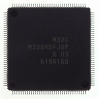
Manufacturer Part Number
M30845FJGP#U3
Description
IC M32C MCU FLASH 512K 144LQFP
Manufacturer
Renesas Electronics America
Series
M16C™ M32C/80r
Specifications of M30845FJGP#U3
Core Processor
M32C/80
Core Size
16/32-Bit
Speed
32MHz
Connectivity
CAN, I²C, IEBus, SIO, UART/USART
Peripherals
DMA, PWM, WDT
Number Of I /o
121
Program Memory Size
512KB (512K x 8)
Program Memory Type
FLASH
Ram Size
24K x 8
Voltage - Supply (vcc/vdd)
3 V ~ 5.5 V
Data Converters
A/D 34x10b, D/A 2x8b
Oscillator Type
Internal
Operating Temperature
-40°C ~ 85°C
Package / Case
144-LQFP
Lead Free Status / RoHS Status
Lead free / RoHS Compliant
Eeprom Size
-
Available stocks
Company
Part Number
Manufacturer
Quantity
Price


M
R
R
e
E
3
8.2 Bus Control
. v
J
2
0
C
Signals, required to access external devices, are provided and software wait states are inserted as follows.
The signals are available in memory expansion mode and microprocessor mode only.
8.2.1 Address Bus and Data Bus
8.2.2 Chip-Select Signal
1
9
8 /
0 .
B
Address bus is a signal accessing 16-Mbyte space and uses 24 control pins; A
inversed output signal of the highest-order address bit.
Data bus is a signal for data input and output. The DS register selects an 8-bit data bus from D
a 16-bit data bus from D
BYTE pin, the data bus accessing the external memory space 3 becomes an 8-bit data bus after reset.
When applying a low-level ("L") signal to the BYTE pin, the data bus accessing the external memory
space 3 becomes the 16-bit data bus.
When changing single-chip mode to memory expansion mode, the address bus is in an indeterminate
state until the microcomputer accesses an external memory space.
Chip-select signal shares pins with A
determine which CS area is accessed and how many chip-select signals are output. A maximum of four
chip-select signals can be output.
In microprocessor mode, no chip-select signal, aside from A
is output after reset.
The chip-select signal becomes "L" while the microcomputer is accessing the external CSi area (i=0 to 3).
It becomes "H" while the microcomputer is accessing other external memory space.
Figure 8.2 shows an example of the address bus and chip-select signal output.
0
1
4
0
G
3
J
6
u
o r
0 -
. l
u
0
1
p
, 7
0
1
(
2
M
0
3
0
2
5
C
8 /
_____
Page 63
, 4
M
3
2
0
C
to D
8 /
f o
4
4
15
) T
9
5
for each external space. When applying a high-level ("H") signal to the
20
to A
22
and A
_____
23
. The PM11 and PM10 bits in the PM1 register
______
23
which can perform as a chip-select signal,
0
to A
22
and A
______
______
23
. A
0
_____
23
to D
is the
8. Bus
7
or
Related parts for M30845FJGP#U3
Image
Part Number
Description
Manufacturer
Datasheet
Request
R

Part Number:
Description:
KIT STARTER FOR M16C/29
Manufacturer:
Renesas Electronics America
Datasheet:

Part Number:
Description:
KIT STARTER FOR R8C/2D
Manufacturer:
Renesas Electronics America
Datasheet:

Part Number:
Description:
R0K33062P STARTER KIT
Manufacturer:
Renesas Electronics America
Datasheet:

Part Number:
Description:
KIT STARTER FOR R8C/23 E8A
Manufacturer:
Renesas Electronics America
Datasheet:

Part Number:
Description:
KIT STARTER FOR R8C/25
Manufacturer:
Renesas Electronics America
Datasheet:

Part Number:
Description:
KIT STARTER H8S2456 SHARPE DSPLY
Manufacturer:
Renesas Electronics America
Datasheet:

Part Number:
Description:
KIT STARTER FOR R8C38C
Manufacturer:
Renesas Electronics America
Datasheet:

Part Number:
Description:
KIT STARTER FOR R8C35C
Manufacturer:
Renesas Electronics America
Datasheet:

Part Number:
Description:
KIT STARTER FOR R8CL3AC+LCD APPS
Manufacturer:
Renesas Electronics America
Datasheet:
Part Number:
Description:
KIT STARTER FOR RX610
Manufacturer:
Renesas Electronics America
Datasheet:

Part Number:
Description:
KIT STARTER FOR R32C/118
Manufacturer:
Renesas Electronics America
Datasheet:

Part Number:
Description:
KIT DEV RSK-R8C/26-29
Manufacturer:
Renesas Electronics America
Datasheet:

Part Number:
Description:
KIT STARTER FOR SH7124
Manufacturer:
Renesas Electronics America
Datasheet:

Part Number:
Description:
KIT STARTER FOR H8SX/1622
Manufacturer:
Renesas Electronics America
Datasheet:

Part Number:
Description:
KIT DEV FOR SH7203
Manufacturer:
Renesas Electronics America
Datasheet: