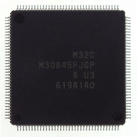
M30845FJGP#U3 Renesas Electronics America, M30845FJGP#U3 Datasheet - Page 83

M30845FJGP#U3
Manufacturer Part Number
M30845FJGP#U3
Description
IC M32C MCU FLASH 512K 144LQFP
Manufacturer
Renesas Electronics America
Series
M16C™ M32C/80r
Specifications of M30845FJGP#U3
Core Processor
M32C/80
Core Size
16/32-Bit
Speed
32MHz
Connectivity
CAN, I²C, IEBus, SIO, UART/USART
Peripherals
DMA, PWM, WDT
Number Of I /o
121
Program Memory Size
512KB (512K x 8)
Program Memory Type
FLASH
Ram Size
24K x 8
Voltage - Supply (vcc/vdd)
3 V ~ 5.5 V
Data Converters
A/D 34x10b, D/A 2x8b
Oscillator Type
Internal
Operating Temperature
-40°C ~ 85°C
Package / Case
144-LQFP
Lead Free Status / RoHS Status
Lead free / RoHS Compliant
Eeprom Size
-
Available stocks
Company
Part Number
Manufacturer
Quantity
Price
- Current page: 83 of 531
- Download datasheet (4Mb)
M
R
R
8. Bus
8.1 Bus Settings
e
E
3
. v
J
2
Table 8.1 Bus Settings
Figure 8.1 DS Register
0
Selecting External Address Bus Width
Setting Bus Width after Reset
Selecting Between Separate Bus or Multiplexed Bus
Number of Chip-Select
C
In memory expansion mode or microprocessor mode, some pins function as bus control pins to control the
address bus and data bus. A
HLDA/ALE, HOLD, ALE, RDY are used as bus control pins.
The BYTE pin, the DS register, the PM05 and PM04 bits in the PM0 register and the PM11 and PM10 bits
in the PM1 register determine bus settings.
Table 8.1 lists how to change bus settings. Figure 8.1 shows the DS register.
1
_________
9
0 .
8 /
B
Bus control pins in M32C/84T cannot be used.
0
1
NOTE
4
0
3
G
J
External Data Bus Width Control Register
6
u
b7
o r
NOTES:
0 -
. l
u
0
1
b6
1. The DS register in M32C/84T cannot be used.
p
, 7
0
1
(
_________
b5
2
M
0
3
0
b4
5
2
C
b3
8 /
Page 60
, 4
b2
Bus Setting
M
b1
3
_______
2
b0
C
0
f o
8 /
(b7 - b4)
Symbol
to A
4
4
DS0
DS1
DS3
Bit
DS2
) T
9
Symbol
DS
5
22
, A
_____
External Space 0 Data
Bus Width Select Bit
External Space 1 Data
Bus Width Select Bit
External Space 3 Data
Bus Width Select Bit
Nothing is assigned. When write, set to "0".
When read, its content is indeterminate.
External Space 2 Data
Bus Width Select Bit
23
, D
0
Bit Name
to D
Address
000B
15
16
, CS0 to CS3, WRL/WR, WRH/BHE, RD, BCLK/ALE,
______
(1)
DS register
BYTE pin (external space 3 only)
PM05 and PM04 bits in PM0 register
PM11 and PM10 bits in PM1 register
0 : 8 bits wide
1 : 16 bits wide
0 : 8 bits wide
1 : 16 bits wide
0 : 8 bits wide
1 : 16 bits wide
0 : 8 bits wide
1 : 16 bits wide
______
______ ___ ______ _________ _______
After Reset
XXXX 1000
XXXX 0000
Function
Changed By
2
2
(BYTE pin = "L")
(BYTE pin = "H")
_____
RW
RW
RW
RW
RW
8. Bus
Related parts for M30845FJGP#U3
Image
Part Number
Description
Manufacturer
Datasheet
Request
R

Part Number:
Description:
KIT STARTER FOR M16C/29
Manufacturer:
Renesas Electronics America
Datasheet:

Part Number:
Description:
KIT STARTER FOR R8C/2D
Manufacturer:
Renesas Electronics America
Datasheet:

Part Number:
Description:
R0K33062P STARTER KIT
Manufacturer:
Renesas Electronics America
Datasheet:

Part Number:
Description:
KIT STARTER FOR R8C/23 E8A
Manufacturer:
Renesas Electronics America
Datasheet:

Part Number:
Description:
KIT STARTER FOR R8C/25
Manufacturer:
Renesas Electronics America
Datasheet:

Part Number:
Description:
KIT STARTER H8S2456 SHARPE DSPLY
Manufacturer:
Renesas Electronics America
Datasheet:

Part Number:
Description:
KIT STARTER FOR R8C38C
Manufacturer:
Renesas Electronics America
Datasheet:

Part Number:
Description:
KIT STARTER FOR R8C35C
Manufacturer:
Renesas Electronics America
Datasheet:

Part Number:
Description:
KIT STARTER FOR R8CL3AC+LCD APPS
Manufacturer:
Renesas Electronics America
Datasheet:

Part Number:
Description:
KIT STARTER FOR RX610
Manufacturer:
Renesas Electronics America
Datasheet:

Part Number:
Description:
KIT STARTER FOR R32C/118
Manufacturer:
Renesas Electronics America
Datasheet:

Part Number:
Description:
KIT DEV RSK-R8C/26-29
Manufacturer:
Renesas Electronics America
Datasheet:

Part Number:
Description:
KIT STARTER FOR SH7124
Manufacturer:
Renesas Electronics America
Datasheet:

Part Number:
Description:
KIT STARTER FOR H8SX/1622
Manufacturer:
Renesas Electronics America
Datasheet:

Part Number:
Description:
KIT DEV FOR SH7203
Manufacturer:
Renesas Electronics America
Datasheet:


