M30845FJGP#U3 Renesas Electronics America, M30845FJGP#U3 Datasheet - Page 274
M30845FJGP#U3
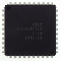
Manufacturer Part Number
M30845FJGP#U3
Description
IC M32C MCU FLASH 512K 144LQFP
Manufacturer
Renesas Electronics America
Series
M16C™ M32C/80r
Specifications of M30845FJGP#U3
Core Processor
M32C/80
Core Size
16/32-Bit
Speed
32MHz
Connectivity
CAN, I²C, IEBus, SIO, UART/USART
Peripherals
DMA, PWM, WDT
Number Of I /o
121
Program Memory Size
512KB (512K x 8)
Program Memory Type
FLASH
Ram Size
24K x 8
Voltage - Supply (vcc/vdd)
3 V ~ 5.5 V
Data Converters
A/D 34x10b, D/A 2x8b
Oscillator Type
Internal
Operating Temperature
-40°C ~ 85°C
Package / Case
144-LQFP
Lead Free Status / RoHS Status
Lead free / RoHS Compliant
Eeprom Size
-
Available stocks
Company
Part Number
Manufacturer
Quantity
Price


M
R
R
e
E
3
. v
J
2
Figure 18.4 AD0CON2 Register
0
C
1
9
8 /
0 .
B
0
1
4
0
G
3
J
6
u
o r
0 -
. l
A/D0 Control Register 2
0 0
b7
u
NOTES:
0
1
p
, 7
0
1. When the AD0CON2 register is rewritten during the A/D conversion, the conversion result is
2. When the MSS bit in the AD0CON3 register is set to "1" (multi-port sweep mode enabled), set the
3. The APS1 and APS0 bits can be set to "01
4. The APS1 and APS0 bits can be set to "10
b6
1
(
2
M
indeterminate.
APS1 and APS0 bits to "01
AD0CON3 register is set to "1" (multi-port sweep mode enabled).
0
b5
3
0
2
5
b4
C
8 /
Page 251
b3
, 4
b2
M
3
b1
2
C
b0
8 /
f o
4
(b4 - b3)
(b7 - b6)
4
Symbol
) T
TRG0
APS0
APS1
9
SMP
Bit
5
2
Symbol
AD0CON2
".
(1)
A/D Conversion
Method Select Bit
Analog Input Port
Select Bit
Nothing is assigned. When write, set to "0".
When read, its content is indeterminate.
External Trigger
Request Cause
Select Bit
Reserved Bit
Bit Name
2
2
" in the 100-pin package only when the MSS bit in the
" or "11
(2, 3, 4)
2
Address
0394
" in single-chip mode only.
16
b2b1
0 : Without the sample and hold funtion
1 : With the sample and hold function
0 0 : AN
0 1 : AN15
1 0 : AN0
1 1 : AN2
0 : Selects AD
1 : Selects a timer B2 interrupt request
Set to "0".
When read, its content is indeterminate.
of the three-phase motor control
timer functions (after the ICTB2
counter completes counting)
0
0
0
to AN
0
to AN0
to AN2
to AN15
TRG
After Reset
XX0X X000
7
, ANEX0, ANEX1
Function
7
7
7
2
18. A/D Converter
RW
RW
RW
RW
RW
RW
Related parts for M30845FJGP#U3
Image
Part Number
Description
Manufacturer
Datasheet
Request
R

Part Number:
Description:
KIT STARTER FOR M16C/29
Manufacturer:
Renesas Electronics America
Datasheet:

Part Number:
Description:
KIT STARTER FOR R8C/2D
Manufacturer:
Renesas Electronics America
Datasheet:

Part Number:
Description:
R0K33062P STARTER KIT
Manufacturer:
Renesas Electronics America
Datasheet:

Part Number:
Description:
KIT STARTER FOR R8C/23 E8A
Manufacturer:
Renesas Electronics America
Datasheet:

Part Number:
Description:
KIT STARTER FOR R8C/25
Manufacturer:
Renesas Electronics America
Datasheet:

Part Number:
Description:
KIT STARTER H8S2456 SHARPE DSPLY
Manufacturer:
Renesas Electronics America
Datasheet:

Part Number:
Description:
KIT STARTER FOR R8C38C
Manufacturer:
Renesas Electronics America
Datasheet:

Part Number:
Description:
KIT STARTER FOR R8C35C
Manufacturer:
Renesas Electronics America
Datasheet:

Part Number:
Description:
KIT STARTER FOR R8CL3AC+LCD APPS
Manufacturer:
Renesas Electronics America
Datasheet:
Part Number:
Description:
KIT STARTER FOR RX610
Manufacturer:
Renesas Electronics America
Datasheet:

Part Number:
Description:
KIT STARTER FOR R32C/118
Manufacturer:
Renesas Electronics America
Datasheet:

Part Number:
Description:
KIT DEV RSK-R8C/26-29
Manufacturer:
Renesas Electronics America
Datasheet:

Part Number:
Description:
KIT STARTER FOR SH7124
Manufacturer:
Renesas Electronics America
Datasheet:

Part Number:
Description:
KIT STARTER FOR H8SX/1622
Manufacturer:
Renesas Electronics America
Datasheet:

Part Number:
Description:
KIT DEV FOR SH7203
Manufacturer:
Renesas Electronics America
Datasheet: