M30845FJGP#U3 Renesas Electronics America, M30845FJGP#U3 Datasheet - Page 6
M30845FJGP#U3
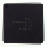
Manufacturer Part Number
M30845FJGP#U3
Description
IC M32C MCU FLASH 512K 144LQFP
Manufacturer
Renesas Electronics America
Series
M16C™ M32C/80r
Specifications of M30845FJGP#U3
Core Processor
M32C/80
Core Size
16/32-Bit
Speed
32MHz
Connectivity
CAN, I²C, IEBus, SIO, UART/USART
Peripherals
DMA, PWM, WDT
Number Of I /o
121
Program Memory Size
512KB (512K x 8)
Program Memory Type
FLASH
Ram Size
24K x 8
Voltage - Supply (vcc/vdd)
3 V ~ 5.5 V
Data Converters
A/D 34x10b, D/A 2x8b
Oscillator Type
Internal
Operating Temperature
-40°C ~ 85°C
Package / Case
144-LQFP
Lead Free Status / RoHS Status
Lead free / RoHS Compliant
Eeprom Size
-
Available stocks
Company
Part Number
Manufacturer
Quantity
Price


Quick Reference by Address _____________________ B-1
1. Overview _____________________________________ 1
2. Central Processing Unit (CPU) __________________ 19
3. Memory _____________________________________ 22
4. Special Function Registers (SFR)________________ 23
5. Reset _______________________________________ 43
6. Voltage Detection Circuit _______________________ 48
1.1 Applications ................................................................................................................ 1
1.2 Performance Overview .............................................................................................. 2
1.3 Block Diagram ............................................................................................................ 4
1.4 Product Information ................................................................................................... 5
1.5 Pin Assignments and Descriptions .......................................................................... 7
1.6 Pin Description ......................................................................................................... 15
2.1 General Registers .................................................................................................... 20
2.2 High-Speed Interrupt Registers .............................................................................. 21
2.3 DMAC-Associated Registers ................................................................................... 21
5.1 Hardware Reset 1 ..................................................................................................... 43
5.2 Low Voltage Detection Reset (Hardware Reset 2)................................................. 45
5.3 Software Reset ......................................................................................................... 46
5.4 Watchdog Timer Reset ............................................................................................ 46
5.5 Internal Space ........................................................................................................... 47
6.1 Low Voltage Detection Interrupt ............................................................................. 52
6.2 Cold Start-up / Warm Start-up Determine Function .............................................. 54
2.1.1 Data Registers (R0, R1, R2 and R3) ................................................................. 20
2.1.2 Address Registers (A0 and A1) ....................................................................... 20
2.1.3 Static Base Register (SB) ................................................................................. 20
2.1.4 Frame Base Register (FB) ................................................................................ 20
2.1.5 Program Counter (PC) ...................................................................................... 20
2.1.6 Interrupt Table Register (INTB) ........................................................................ 20
2.1.7 User Stack Pointer (USP), Interrupt Stack Pointer (ISP) ............................... 20
2.1.8 Flag Register (FLG) ........................................................................................... 20
5.1.1 Reset on a Stable Supply Voltage .................................................................... 43
5.1.2 Power-on Reset .................................................................................................. 43
6.1.1 Limitations on Exiting Stop/Wait Mode........................................................... 54
Table of Contents
A-1
Related parts for M30845FJGP#U3
Image
Part Number
Description
Manufacturer
Datasheet
Request
R

Part Number:
Description:
KIT STARTER FOR M16C/29
Manufacturer:
Renesas Electronics America
Datasheet:

Part Number:
Description:
KIT STARTER FOR R8C/2D
Manufacturer:
Renesas Electronics America
Datasheet:

Part Number:
Description:
R0K33062P STARTER KIT
Manufacturer:
Renesas Electronics America
Datasheet:

Part Number:
Description:
KIT STARTER FOR R8C/23 E8A
Manufacturer:
Renesas Electronics America
Datasheet:

Part Number:
Description:
KIT STARTER FOR R8C/25
Manufacturer:
Renesas Electronics America
Datasheet:

Part Number:
Description:
KIT STARTER H8S2456 SHARPE DSPLY
Manufacturer:
Renesas Electronics America
Datasheet:

Part Number:
Description:
KIT STARTER FOR R8C38C
Manufacturer:
Renesas Electronics America
Datasheet:

Part Number:
Description:
KIT STARTER FOR R8C35C
Manufacturer:
Renesas Electronics America
Datasheet:

Part Number:
Description:
KIT STARTER FOR R8CL3AC+LCD APPS
Manufacturer:
Renesas Electronics America
Datasheet:
Part Number:
Description:
KIT STARTER FOR RX610
Manufacturer:
Renesas Electronics America
Datasheet:

Part Number:
Description:
KIT STARTER FOR R32C/118
Manufacturer:
Renesas Electronics America
Datasheet:

Part Number:
Description:
KIT DEV RSK-R8C/26-29
Manufacturer:
Renesas Electronics America
Datasheet:

Part Number:
Description:
KIT STARTER FOR SH7124
Manufacturer:
Renesas Electronics America
Datasheet:

Part Number:
Description:
KIT STARTER FOR H8SX/1622
Manufacturer:
Renesas Electronics America
Datasheet:

Part Number:
Description:
KIT DEV FOR SH7203
Manufacturer:
Renesas Electronics America
Datasheet: