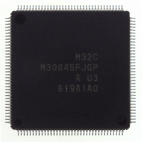
M30845FJGP#U3 Renesas Electronics America, M30845FJGP#U3 Datasheet - Page 401

M30845FJGP#U3
Manufacturer Part Number
M30845FJGP#U3
Description
IC M32C MCU FLASH 512K 144LQFP
Manufacturer
Renesas Electronics America
Series
M16C™ M32C/80r
Specifications of M30845FJGP#U3
Core Processor
M32C/80
Core Size
16/32-Bit
Speed
32MHz
Connectivity
CAN, I²C, IEBus, SIO, UART/USART
Peripherals
DMA, PWM, WDT
Number Of I /o
121
Program Memory Size
512KB (512K x 8)
Program Memory Type
FLASH
Ram Size
24K x 8
Voltage - Supply (vcc/vdd)
3 V ~ 5.5 V
Data Converters
A/D 34x10b, D/A 2x8b
Oscillator Type
Internal
Operating Temperature
-40°C ~ 85°C
Package / Case
144-LQFP
Lead Free Status / RoHS Status
Lead free / RoHS Compliant
Eeprom Size
-
Available stocks
Company
Part Number
Manufacturer
Quantity
Price
- Current page: 401 of 531
- Download datasheet (4Mb)
M
R
R
e
E
3
. v
J
2
Figure 24.6 P0 to P15 Registers
0
C
1
9
0 .
8 /
B
0
1
4
0
3
G
J
6
u
o r
0 -
. l
Port Pi Register
b7
u
0
1
NOTES:
p
, 7
0
b6
1
1. In memory expansion mode and microprocessor mode, the Pi register cannot control pins being used
2. The P11 to P15 registers are provided in the 144-pin package only.
3. P7
4. The P8_5 bit is for read only.
5. Nothing is assigned in the P11_7 to P11_5 bits in the P11 register and the P14_7 bit in the P14
(
2
M
0
as bus control pins (A
BCLK/ALE/CLK
when P7
register. If write, set these bits to "0". When read, their contents are indeterminate.
M32C/84T cannot be used in memory expansion mode and microprocessor mode.
b5
3
0
2
0
5
C
b4
and P7
8 /
Page 378
b3
, 4
0
and P7
b2
1
M
are ports for the N-channel open drain output. The pins go into high-impedance states
3
b1
2
OUT
C
1
b0
(i=0 to 15)
f o
8 /
put in "H" signal outputs.
, HLDA/ALE, HOLD, ALE and RDY).
4
0
4
) T
to A
Symbol
9
Pi_0
Pi_1
Pi_2
Pi_3
Pi_4
Pi_5
Pi_6
Pi_7
Symbol
P0 to P5
P6 to P10
P11 to P15 03C9
5
Bit
22
, A
(1, 2)
23
Port Pi
Port Pi
Port Pi
Port Pi
Port Pi
Port Pi
Port Pi
Port Pi
, D
0
Address
03E0
03C0
to D
0
1
2
3
4
5
6
7
Bit Name
16
16
16 (5)
Bit
Bit
Bit
Bit
Bit
Bit
Bit
Bit
15
, 03E1
, 03C1
, CS0 to CS3, WRL/WR, WRH/BHE, RD,
, 03CC
16
16
, 03E4
(3)
16
, 03C4
, 03CD
16
, 03E5
16
Pin levels can be read by reading
bits corresponding to programmable
ports in input mode.
Pin levels can be controlled by
writing to bits corresponding to
programmable ports in output mode.
0: "L" level
1: "H" level
16
(4)
, 03D0
, 03C5
16
, 03E8
16 (5)
16
, 03C8
, 03D1
16
, 03E9
Function
16
16
16
24. Programmable I/O Ports
After Reset
Indeterminate
Indeterminate
Indeterminate
RW
RW
RW
RW
RW
RW
RW
RW
RW
Related parts for M30845FJGP#U3
Image
Part Number
Description
Manufacturer
Datasheet
Request
R

Part Number:
Description:
KIT STARTER FOR M16C/29
Manufacturer:
Renesas Electronics America
Datasheet:

Part Number:
Description:
KIT STARTER FOR R8C/2D
Manufacturer:
Renesas Electronics America
Datasheet:

Part Number:
Description:
R0K33062P STARTER KIT
Manufacturer:
Renesas Electronics America
Datasheet:

Part Number:
Description:
KIT STARTER FOR R8C/23 E8A
Manufacturer:
Renesas Electronics America
Datasheet:

Part Number:
Description:
KIT STARTER FOR R8C/25
Manufacturer:
Renesas Electronics America
Datasheet:

Part Number:
Description:
KIT STARTER H8S2456 SHARPE DSPLY
Manufacturer:
Renesas Electronics America
Datasheet:

Part Number:
Description:
KIT STARTER FOR R8C38C
Manufacturer:
Renesas Electronics America
Datasheet:

Part Number:
Description:
KIT STARTER FOR R8C35C
Manufacturer:
Renesas Electronics America
Datasheet:

Part Number:
Description:
KIT STARTER FOR R8CL3AC+LCD APPS
Manufacturer:
Renesas Electronics America
Datasheet:

Part Number:
Description:
KIT STARTER FOR RX610
Manufacturer:
Renesas Electronics America
Datasheet:

Part Number:
Description:
KIT STARTER FOR R32C/118
Manufacturer:
Renesas Electronics America
Datasheet:

Part Number:
Description:
KIT DEV RSK-R8C/26-29
Manufacturer:
Renesas Electronics America
Datasheet:

Part Number:
Description:
KIT STARTER FOR SH7124
Manufacturer:
Renesas Electronics America
Datasheet:

Part Number:
Description:
KIT STARTER FOR H8SX/1622
Manufacturer:
Renesas Electronics America
Datasheet:

Part Number:
Description:
KIT DEV FOR SH7203
Manufacturer:
Renesas Electronics America
Datasheet:


