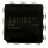
DF61654N50FTV Renesas Electronics America, DF61654N50FTV Datasheet - Page 325

DF61654N50FTV
Manufacturer Part Number
DF61654N50FTV
Description
IC H8SX/1654 MCU FLASH 120TQFP
Manufacturer
Renesas Electronics America
Series
H8® H8SX/1600r
Datasheet
1.DF61653N50FTV.pdf
(1020 pages)
Specifications of DF61654N50FTV
Core Processor
H8SX
Core Size
32-Bit
Speed
50MHz
Connectivity
I²C, IrDA, SCI, SmartCard, USB
Peripherals
DMA, PWM, WDT
Number Of I /o
75
Program Memory Size
512KB (512K x 8)
Program Memory Type
FLASH
Ram Size
40K x 8
Voltage - Supply (vcc/vdd)
3 V ~ 3.6 V
Data Converters
A/D 8x10b; D/A 2x8b
Oscillator Type
External
Operating Temperature
-20°C ~ 75°C
Package / Case
120-TQFP, 120-VQFP
For Use With
HS0005KCU11H - EMULATOR E10A-USB H8S(X),SH2(A)3DK1657 - DEV EVAL KIT FOR H8SX/1657
Lead Free Status / RoHS Status
Lead free / RoHS Compliant
Eeprom Size
-
Available stocks
Company
Part Number
Manufacturer
Quantity
Price
Company:
Part Number:
DF61654N50FTV
Manufacturer:
Renesas Electronics America
Quantity:
10 000
- Current page: 325 of 1020
- Download datasheet (6Mb)
(3)
When setting the negative value in DOFR, the offset value must be 2's complement. The 2's
complement is obtained by the following formula.
Example:
= H'FFFE0000 + H'00000001
= H'FFFE0001
The value of 2's complement can be obtained by the NEG.L instruction.
7.5.7
The DMAC registers are updated by a DMA transfer. The value to be updated differs according to
the other settings and transfer state. The registers to be updated are DSAR, DDAR, DTCR, bits
BKSZH and BKSZ in DBSR, and the DTE, ACT, ERRF, ESIF, and DTIF bits in DMDR.
(1)
When the transfer source address set in DSAR is accessed, the contents of DSAR are output and
then are updated to the next address.
The increment or decrement can be specified by bits SAT1 and SAT0 in DACR. When SAT1 and
SAT0 = B'00, the address is fixed. When SAT1 and SAT0 = B'01, the address is added with the
offset. When SAT1 and SAT0 = B'10, the address is incremented. When SAT1 and SAT0 = B'11,
the address is decremented. The size of increment or decrement depends on the data access size.
The data access size is specified by bits DTSZ1 and DTSZ0 in DMDR. When DTSZ1 and DTSZ0
= B'00, the data access size is byte and the address is incremented or decremented by 1. When
DTSZ1 and DTSZ0 = B'01, the data access size is word and the address is incremented or
decremented by 2. When DTSZ1 and DTSZ0 = B'10, the data access size is longword and the
address is incremented or decremented by 4. Even if the access data size of the source address is
word or longword, when the source address is not aligned with the word or longword boundary,
the read bus cycle is divided into byte or word cycles. While data of one word or one longword is
being read, the size of increment or decrement is changing according to the actual data access size,
for example, +1 or +2 for byte or word data. After one word or one longword of data is read, the
address when the read cycle is started is incremented or decremented by the value according to
bits SAT1 and SAT0.
2's complement of offset = 1 + ~offset (~: bit inversion)
Offset Subtraction
DMA Source Address Register
Register during DMA Transfer
2's complement of H'0001FFFF
Rev.1.00 Sep. 08, 2005 Page 275 of 966
Section 7 DMA Controller (DMAC)
REJ09B0219-0100
Related parts for DF61654N50FTV
Image
Part Number
Description
Manufacturer
Datasheet
Request
R

Part Number:
Description:
KIT STARTER FOR M16C/29
Manufacturer:
Renesas Electronics America
Datasheet:

Part Number:
Description:
KIT STARTER FOR R8C/2D
Manufacturer:
Renesas Electronics America
Datasheet:

Part Number:
Description:
R0K33062P STARTER KIT
Manufacturer:
Renesas Electronics America
Datasheet:

Part Number:
Description:
KIT STARTER FOR R8C/23 E8A
Manufacturer:
Renesas Electronics America
Datasheet:

Part Number:
Description:
KIT STARTER FOR R8C/25
Manufacturer:
Renesas Electronics America
Datasheet:

Part Number:
Description:
KIT STARTER H8S2456 SHARPE DSPLY
Manufacturer:
Renesas Electronics America
Datasheet:

Part Number:
Description:
KIT STARTER FOR R8C38C
Manufacturer:
Renesas Electronics America
Datasheet:

Part Number:
Description:
KIT STARTER FOR R8C35C
Manufacturer:
Renesas Electronics America
Datasheet:

Part Number:
Description:
KIT STARTER FOR R8CL3AC+LCD APPS
Manufacturer:
Renesas Electronics America
Datasheet:

Part Number:
Description:
KIT STARTER FOR RX610
Manufacturer:
Renesas Electronics America
Datasheet:

Part Number:
Description:
KIT STARTER FOR R32C/118
Manufacturer:
Renesas Electronics America
Datasheet:

Part Number:
Description:
KIT DEV RSK-R8C/26-29
Manufacturer:
Renesas Electronics America
Datasheet:

Part Number:
Description:
KIT STARTER FOR SH7124
Manufacturer:
Renesas Electronics America
Datasheet:

Part Number:
Description:
KIT STARTER FOR H8SX/1622
Manufacturer:
Renesas Electronics America
Datasheet:

Part Number:
Description:
KIT DEV FOR SH7203
Manufacturer:
Renesas Electronics America
Datasheet:


