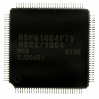
DF61654N50FTV Renesas Electronics America, DF61654N50FTV Datasheet - Page 551

DF61654N50FTV
Manufacturer Part Number
DF61654N50FTV
Description
IC H8SX/1654 MCU FLASH 120TQFP
Manufacturer
Renesas Electronics America
Series
H8® H8SX/1600r
Datasheet
1.DF61653N50FTV.pdf
(1020 pages)
Specifications of DF61654N50FTV
Core Processor
H8SX
Core Size
32-Bit
Speed
50MHz
Connectivity
I²C, IrDA, SCI, SmartCard, USB
Peripherals
DMA, PWM, WDT
Number Of I /o
75
Program Memory Size
512KB (512K x 8)
Program Memory Type
FLASH
Ram Size
40K x 8
Voltage - Supply (vcc/vdd)
3 V ~ 3.6 V
Data Converters
A/D 8x10b; D/A 2x8b
Oscillator Type
External
Operating Temperature
-20°C ~ 75°C
Package / Case
120-TQFP, 120-VQFP
For Use With
HS0005KCU11H - EMULATOR E10A-USB H8S(X),SH2(A)3DK1657 - DEV EVAL KIT FOR H8SX/1657
Lead Free Status / RoHS Status
Lead free / RoHS Compliant
Eeprom Size
-
Available stocks
Company
Part Number
Manufacturer
Quantity
Price
Company:
Part Number:
DF61654N50FTV
Manufacturer:
Renesas Electronics America
Quantity:
10 000
- Current page: 551 of 1020
- Download datasheet (6Mb)
This LSI has four units (unit 0 to unit 3) of an on-chip 8-bit timer module that comprise two 8-bit
counter channels, totaling eight channels. The 8-bit timer module can be used to count external
events and also be used as a multifunction timer in a variety of applications, such as generation of
counter reset, interrupt requests, and pulse output with a desired duty cycle using a compare-match
signal with two registers.
Figures 12.1 to 12.4 show block diagrams of the 8-bit timer module (unit 0 to unit 3).
This section describes unit 0 (channels 0 and 1) and unit 2 (channels 4 and 5), both of which have
the same functions. Unit2 and unit 3 can generate baud rate clock for SCI and have the same
functions.
12.1
• Selection of seven clock sources
• Selection of three ways to clear the counters
• Timer output control by a combination of two compare match signals
• Cascading of two channels
• Three interrupt sources
• Generation of trigger to start A/D converter conversion (available in unit 0 and unit 1 only)
• Capable of generating baud rate clock for SCI_5 and SCI_6. (This is available only in unit 2
The counters can be driven by one of six internal clock signals (Pφ/2, Pφ/8, Pφ/32, Pφ/64,
Pφ/1024, or Pφ/8192) or an external clock input (only internal clock available in units 2 and 3:
Pφ, Pφ/2, Pφ/8, Pφ/32, Pφ/64, Pφ/1024, and Pφ/8192).
The counters can be cleared on compare match A or B, or by an external reset signal. (This is
available only in unit 0 and unit 1.)
The timer output signal in each channel is controlled by a combination of two independent
compare match signals, enabling the timer to output pulses with a desired duty cycle or PWM
output.
Operation as a 16-bit timer is possible, using TMR_0 for the upper 8 bits and TMR_1 for the
lower 8 bits (16-bit count mode).
TMR_1 can be used to count TMR_0 compare matches (compare match count mode).
Compare match A, compare match B, and overflow interrupts can be requested independently.
(This is available only in unit 0 and unit 1.)
and unit 3.)For details, see section 14, Serial Communication Interface (SCI).
Features
Section 12 8-Bit Timers (TMR)
Rev.1.00 Sep. 08, 2005 Page 501 of 966
Section 12 8-Bit Timers (TMR)
REJ09B0219-0100
Related parts for DF61654N50FTV
Image
Part Number
Description
Manufacturer
Datasheet
Request
R

Part Number:
Description:
KIT STARTER FOR M16C/29
Manufacturer:
Renesas Electronics America
Datasheet:

Part Number:
Description:
KIT STARTER FOR R8C/2D
Manufacturer:
Renesas Electronics America
Datasheet:

Part Number:
Description:
R0K33062P STARTER KIT
Manufacturer:
Renesas Electronics America
Datasheet:

Part Number:
Description:
KIT STARTER FOR R8C/23 E8A
Manufacturer:
Renesas Electronics America
Datasheet:

Part Number:
Description:
KIT STARTER FOR R8C/25
Manufacturer:
Renesas Electronics America
Datasheet:

Part Number:
Description:
KIT STARTER H8S2456 SHARPE DSPLY
Manufacturer:
Renesas Electronics America
Datasheet:

Part Number:
Description:
KIT STARTER FOR R8C38C
Manufacturer:
Renesas Electronics America
Datasheet:

Part Number:
Description:
KIT STARTER FOR R8C35C
Manufacturer:
Renesas Electronics America
Datasheet:

Part Number:
Description:
KIT STARTER FOR R8CL3AC+LCD APPS
Manufacturer:
Renesas Electronics America
Datasheet:

Part Number:
Description:
KIT STARTER FOR RX610
Manufacturer:
Renesas Electronics America
Datasheet:

Part Number:
Description:
KIT STARTER FOR R32C/118
Manufacturer:
Renesas Electronics America
Datasheet:

Part Number:
Description:
KIT DEV RSK-R8C/26-29
Manufacturer:
Renesas Electronics America
Datasheet:

Part Number:
Description:
KIT STARTER FOR SH7124
Manufacturer:
Renesas Electronics America
Datasheet:

Part Number:
Description:
KIT STARTER FOR H8SX/1622
Manufacturer:
Renesas Electronics America
Datasheet:

Part Number:
Description:
KIT DEV FOR SH7203
Manufacturer:
Renesas Electronics America
Datasheet:


