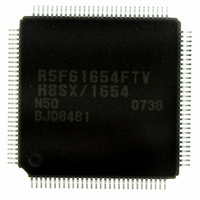
DF61654N50FTV Renesas Electronics America, DF61654N50FTV Datasheet - Page 977

DF61654N50FTV
Manufacturer Part Number
DF61654N50FTV
Description
IC H8SX/1654 MCU FLASH 120TQFP
Manufacturer
Renesas Electronics America
Series
H8® H8SX/1600r
Datasheet
1.DF61653N50FTV.pdf
(1020 pages)
Specifications of DF61654N50FTV
Core Processor
H8SX
Core Size
32-Bit
Speed
50MHz
Connectivity
I²C, IrDA, SCI, SmartCard, USB
Peripherals
DMA, PWM, WDT
Number Of I /o
75
Program Memory Size
512KB (512K x 8)
Program Memory Type
FLASH
Ram Size
40K x 8
Voltage - Supply (vcc/vdd)
3 V ~ 3.6 V
Data Converters
A/D 8x10b; D/A 2x8b
Oscillator Type
External
Operating Temperature
-20°C ~ 75°C
Package / Case
120-TQFP, 120-VQFP
For Use With
HS0005KCU11H - EMULATOR E10A-USB H8S(X),SH2(A)3DK1657 - DEV EVAL KIT FOR H8SX/1657
Lead Free Status / RoHS Status
Lead free / RoHS Compliant
Eeprom Size
-
Available stocks
Company
Part Number
Manufacturer
Quantity
Price
Company:
Part Number:
DF61654N50FTV
Manufacturer:
Renesas Electronics America
Quantity:
10 000
- Current page: 977 of 1020
- Download datasheet (6Mb)
Table 24.6 Bus Timing (2)
Conditions: V
Item
WR delay time 1
WR delay time 2
WR pulse width 1
WR pulse width 2
Write data delay time
Write data setup time 1
Write data setup time 2
Write data setup time 3
Write data hold time 1
Write data hold time 3
Byte control delay time
Byte control pulse width 1
Byte control pulse width 2
Multiplexed address delay time 1
Multiplexed address hold time
Multiplexed address setup time 1
Multiplexed address setup time 2
Address hold delay time
Address hold pulse width 1
Address hold pulse width 2
WAIT setup time
WAIT hold time
BREQ setup time
BACK delay time
Bus floating time
BREQO delay time
BS delay time
RD/WR delay time
V
T
T
a
a
CC
SS
= –20°C to +75°C (regular specifications),
= –40°C to +85°C (wide-range specifications)
= PLLV
= PLLV
SS
CC
= DrV
= DrV
Symbol
t
t
t
t
t
t
t
t
t
t
t
t
t
t
t
t
t
t
t
t
t
t
t
t
t
t
T
T
SS
WRD1
WRD2
WSW1
WSW2
WDD
WDS1
WDS2
WDS3
WDH1
WDH3
UBD
UBW1
UBW2
MAD1
MAH
MAS1
MAS2
AHD
AHW1
AHW2
WTS
WTH
BREQS
BACD
BZD
BRQOD
CC
BSD
RWD
= AV
= 3.0 V to 3.6 V, AV
SS
= 0 V, Bφ = 8 MHz to 50 MHz,
Min.
1.0 × t
1.5 × t
0.5 × t
1.0 × t
1.5 × t
0.5 × t
1.5 × t
1.0 × t
0.5 × t
1.5 × t
1.0 × t
2.0 × t
15
5.0
20
1.0
CYC
CYC
CYC
CYC
CYC
CYC
CYC
CYC
CYC
CYC
CYC
CYC
– 13
– 13
– 13
– 13
– 13
– 8
– 8
– 15
– 15
– 15
– 15
– 15
CC
Max.
15
15
20
15
1.0 × t
2.0 × t
18
15
15
30
15
15
15
= 3.0 V to 3.6 V, V
Rev.1.00 Sep. 08, 2005 Page 927 of 966
Section 24 Electrical Characteristics
CYC
CYC
– 15 ns
– 15 ns
Unit
ns
ns
ns
ns
ns
ns
ns
ns
ns
ns
ns
ns
ns
ns
ns
ns
ns
ns
ns
ns
ns
ns
ns
ns
ns
ns
ref
= 3.0 V to AV
REJ09B0219-0100
Test
Conditions
24.14
Figures 24.17,
24.18
Figures 24.10,
24.18
Figure 24.19
Figures 24.8,
24.9, 24.11 to
24.14
Figures 24.8 to
24.20
Figures 24.13,
Figure 24.13
Figure 24.14
Figure 24.20
CC
,
Related parts for DF61654N50FTV
Image
Part Number
Description
Manufacturer
Datasheet
Request
R

Part Number:
Description:
KIT STARTER FOR M16C/29
Manufacturer:
Renesas Electronics America
Datasheet:

Part Number:
Description:
KIT STARTER FOR R8C/2D
Manufacturer:
Renesas Electronics America
Datasheet:

Part Number:
Description:
R0K33062P STARTER KIT
Manufacturer:
Renesas Electronics America
Datasheet:

Part Number:
Description:
KIT STARTER FOR R8C/23 E8A
Manufacturer:
Renesas Electronics America
Datasheet:

Part Number:
Description:
KIT STARTER FOR R8C/25
Manufacturer:
Renesas Electronics America
Datasheet:

Part Number:
Description:
KIT STARTER H8S2456 SHARPE DSPLY
Manufacturer:
Renesas Electronics America
Datasheet:

Part Number:
Description:
KIT STARTER FOR R8C38C
Manufacturer:
Renesas Electronics America
Datasheet:

Part Number:
Description:
KIT STARTER FOR R8C35C
Manufacturer:
Renesas Electronics America
Datasheet:

Part Number:
Description:
KIT STARTER FOR R8CL3AC+LCD APPS
Manufacturer:
Renesas Electronics America
Datasheet:

Part Number:
Description:
KIT STARTER FOR RX610
Manufacturer:
Renesas Electronics America
Datasheet:

Part Number:
Description:
KIT STARTER FOR R32C/118
Manufacturer:
Renesas Electronics America
Datasheet:

Part Number:
Description:
KIT DEV RSK-R8C/26-29
Manufacturer:
Renesas Electronics America
Datasheet:

Part Number:
Description:
KIT STARTER FOR SH7124
Manufacturer:
Renesas Electronics America
Datasheet:

Part Number:
Description:
KIT STARTER FOR H8SX/1622
Manufacturer:
Renesas Electronics America
Datasheet:

Part Number:
Description:
KIT DEV FOR SH7203
Manufacturer:
Renesas Electronics America
Datasheet:


