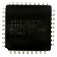
DF61654N50FTV Renesas Electronics America, DF61654N50FTV Datasheet - Page 34

DF61654N50FTV
Manufacturer Part Number
DF61654N50FTV
Description
IC H8SX/1654 MCU FLASH 120TQFP
Manufacturer
Renesas Electronics America
Series
H8® H8SX/1600r
Datasheet
1.DF61653N50FTV.pdf
(1020 pages)
Specifications of DF61654N50FTV
Core Processor
H8SX
Core Size
32-Bit
Speed
50MHz
Connectivity
I²C, IrDA, SCI, SmartCard, USB
Peripherals
DMA, PWM, WDT
Number Of I /o
75
Program Memory Size
512KB (512K x 8)
Program Memory Type
FLASH
Ram Size
40K x 8
Voltage - Supply (vcc/vdd)
3 V ~ 3.6 V
Data Converters
A/D 8x10b; D/A 2x8b
Oscillator Type
External
Operating Temperature
-20°C ~ 75°C
Package / Case
120-TQFP, 120-VQFP
For Use With
HS0005KCU11H - EMULATOR E10A-USB H8S(X),SH2(A)3DK1657 - DEV EVAL KIT FOR H8SX/1657
Lead Free Status / RoHS Status
Lead free / RoHS Compliant
Eeprom Size
-
Available stocks
Company
Part Number
Manufacturer
Quantity
Price
Company:
Part Number:
DF61654N50FTV
Manufacturer:
Renesas Electronics America
Quantity:
10 000
- Current page: 34 of 1020
- Download datasheet (6Mb)
Figure 10.28 Example of Phase Counting Mode 4 Operation .................................................... 458
Figure 10.29 Phase Counting Mode Application Example......................................................... 460
Figure 10.30 Count Timing in Internal Clock Operation............................................................ 464
Figure 10.31 Count Timing in External Clock Operation .......................................................... 464
Figure 10.32 Output Compare Output Timing ........................................................................... 465
Figure 10.33 Input Capture Input Signal Timing........................................................................ 465
Figure 10.34 Counter Clear Timing (Compare Match) .............................................................. 466
Figure 10.35 Counter Clear Timing (Input Capture) .................................................................. 466
Figure 10.36 Buffer Operation Timing (Compare Match) ......................................................... 467
Figure 10.37 Buffer Operation Timing (Input Capture) ............................................................. 467
Figure 10.38 TGI Interrupt Timing (Compare Match) ............................................................... 468
Figure 10.39 TGI Interrupt Timing (Input Capture) ................................................................... 468
Figure 10.40 TCIV Interrupt Setting Timing.............................................................................. 469
Figure 10.41 TCIU Interrupt Setting Timing.............................................................................. 469
Figure 10.42 Timing for Status Flag Clearing by CPU .............................................................. 470
Figure 10.43 Timing for Status Flag Clearing by DTC or DMAC Activation (1)...................... 471
Figure 10.44 Timing for Status Flag Clearing by DTC or DMAC Activation (2)...................... 471
Figure 10.45 Phase Difference, Overlap, and Pulse Width in Phase Counting Mode ................ 472
Figure 10.46 Conflict between TCNT Write and Clear Operations ........................................... 473
Figure 10.47 Conflict between TCNT Write and Increment Operations.................................... 474
Figure 10.48 Conflict between TGR Write and Compare Match ............................................... 474
Figure 10.49 Conflict between Buffer Register Write and Compare Match .............................. 475
Figure 10.50 Conflict between TGR Read and Input Capture.................................................... 476
Figure 10.51 Conflict between TGR Write and Input Capture................................................... 476
Figure 10.52 Conflict between Buffer Register Write and Input Capture .................................. 477
Figure 10.53 Conflict between Overflow and Counter Clearing ................................................ 478
Figure 10.54 Conflict between TCNT Write and Overflow ....................................................... 478
Section 11 Programmable Pulse Generator (PPG)
Figure 11.1 Block Diagram of PPG............................................................................................ 479
Figure 11.2 Schematic Diagram of PPG..................................................................................... 488
Figure 11.3 Timing of Transfer and Output of NDR Contents (Example) ................................. 489
Figure 11.4 Setup Procedure for Normal Pulse Output (Example) ............................................ 490
Figure 11.5 Normal Pulse Output Example (5-Phase Pulse Output) .......................................... 491
Figure 11.6 Non-Overlapping Pulse Output ............................................................................... 492
Figure 11.7 Non-Overlapping Operation and NDR Write Timing ............................................. 493
Figure 11.8 Setup Procedure for Non-Overlapping Pulse Output (Example)............................. 494
Figure 11.9 Non-Overlapping Pulse Output Example (4-Phase Complementary) ..................... 495
Figure 11.10 Inverted Pulse Output (Example) .......................................................................... 497
Figure 11.11 Pulse Output Triggered by Input Capture (Example)............................................ 498
Rev.1.00 Sep. 08, 2005 Page xxxii of xlviii
Related parts for DF61654N50FTV
Image
Part Number
Description
Manufacturer
Datasheet
Request
R

Part Number:
Description:
KIT STARTER FOR M16C/29
Manufacturer:
Renesas Electronics America
Datasheet:

Part Number:
Description:
KIT STARTER FOR R8C/2D
Manufacturer:
Renesas Electronics America
Datasheet:

Part Number:
Description:
R0K33062P STARTER KIT
Manufacturer:
Renesas Electronics America
Datasheet:

Part Number:
Description:
KIT STARTER FOR R8C/23 E8A
Manufacturer:
Renesas Electronics America
Datasheet:

Part Number:
Description:
KIT STARTER FOR R8C/25
Manufacturer:
Renesas Electronics America
Datasheet:

Part Number:
Description:
KIT STARTER H8S2456 SHARPE DSPLY
Manufacturer:
Renesas Electronics America
Datasheet:

Part Number:
Description:
KIT STARTER FOR R8C38C
Manufacturer:
Renesas Electronics America
Datasheet:

Part Number:
Description:
KIT STARTER FOR R8C35C
Manufacturer:
Renesas Electronics America
Datasheet:

Part Number:
Description:
KIT STARTER FOR R8CL3AC+LCD APPS
Manufacturer:
Renesas Electronics America
Datasheet:

Part Number:
Description:
KIT STARTER FOR RX610
Manufacturer:
Renesas Electronics America
Datasheet:

Part Number:
Description:
KIT STARTER FOR R32C/118
Manufacturer:
Renesas Electronics America
Datasheet:

Part Number:
Description:
KIT DEV RSK-R8C/26-29
Manufacturer:
Renesas Electronics America
Datasheet:

Part Number:
Description:
KIT STARTER FOR SH7124
Manufacturer:
Renesas Electronics America
Datasheet:

Part Number:
Description:
KIT STARTER FOR H8SX/1622
Manufacturer:
Renesas Electronics America
Datasheet:

Part Number:
Description:
KIT DEV FOR SH7203
Manufacturer:
Renesas Electronics America
Datasheet:


