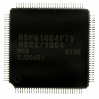
DF61654N50FTV Renesas Electronics America, DF61654N50FTV Datasheet - Page 678

DF61654N50FTV
Manufacturer Part Number
DF61654N50FTV
Description
IC H8SX/1654 MCU FLASH 120TQFP
Manufacturer
Renesas Electronics America
Series
H8® H8SX/1600r
Datasheet
1.DF61653N50FTV.pdf
(1020 pages)
Specifications of DF61654N50FTV
Core Processor
H8SX
Core Size
32-Bit
Speed
50MHz
Connectivity
I²C, IrDA, SCI, SmartCard, USB
Peripherals
DMA, PWM, WDT
Number Of I /o
75
Program Memory Size
512KB (512K x 8)
Program Memory Type
FLASH
Ram Size
40K x 8
Voltage - Supply (vcc/vdd)
3 V ~ 3.6 V
Data Converters
A/D 8x10b; D/A 2x8b
Oscillator Type
External
Operating Temperature
-20°C ~ 75°C
Package / Case
120-TQFP, 120-VQFP
For Use With
HS0005KCU11H - EMULATOR E10A-USB H8S(X),SH2(A)3DK1657 - DEV EVAL KIT FOR H8SX/1657
Lead Free Status / RoHS Status
Lead free / RoHS Compliant
Eeprom Size
-
Available stocks
Company
Part Number
Manufacturer
Quantity
Price
Company:
Part Number:
DF61654N50FTV
Manufacturer:
Renesas Electronics America
Quantity:
10 000
- Current page: 678 of 1020
- Download datasheet (6Mb)
Section 14 Serial Communication Interface (SCI, IrDA, CRC)
14.10.5 Relation between Writing to TDR and TDRE Flag
The TDRE flag in SSR is a status flag which indicates that transmit data has been transferred from
TDR to TSR. When the SCI transfers data from TDR to TSR, the TDRE flag is set to 1.
Data can be written to TDR irrespective of the TDRE flag status. However, if new data is written
to TDR when the TDRE flag is 0, that is, when the previous data has not been transferred to TSR
yet, the previous data in TDR is lost. Be sure to write transmit data to TDR after verifying that the
TDRE flag is set to 1.
14.10.6 Restrictions on Using DTC or DMAC
• When the external clock source is used as a synchronization clock, update TDR by the DMAC
• When using the DMAC or DTC to read RDR, be sure to set the receive end interrupt (RXI) as
• The DTC is not activated by the RXI or TXI request by SCI_5 or SCI6.
Rev.1.00 Sep. 08, 2005 Page 628 of 966
REJ09B0219-0100
or DTC and wait for at least five Pφ clock cycles before allowing the transmit clock to be
input. If the transmit clock is input within four clock cycles after TDR modification, the SCI
may malfunction (see figure 14.38).
the DTC or DMAC activation source.
Figure 14.38 Sample Transmission using DTC in Clocked Synchronous Mode
SCK
TDRE
Serial data
Note: When external clock is supplied, t must be more than four clock cycles.
t
LSB
D0
D1
D2
D3
D4
D5
D6
D7
Related parts for DF61654N50FTV
Image
Part Number
Description
Manufacturer
Datasheet
Request
R

Part Number:
Description:
KIT STARTER FOR M16C/29
Manufacturer:
Renesas Electronics America
Datasheet:

Part Number:
Description:
KIT STARTER FOR R8C/2D
Manufacturer:
Renesas Electronics America
Datasheet:

Part Number:
Description:
R0K33062P STARTER KIT
Manufacturer:
Renesas Electronics America
Datasheet:

Part Number:
Description:
KIT STARTER FOR R8C/23 E8A
Manufacturer:
Renesas Electronics America
Datasheet:

Part Number:
Description:
KIT STARTER FOR R8C/25
Manufacturer:
Renesas Electronics America
Datasheet:

Part Number:
Description:
KIT STARTER H8S2456 SHARPE DSPLY
Manufacturer:
Renesas Electronics America
Datasheet:

Part Number:
Description:
KIT STARTER FOR R8C38C
Manufacturer:
Renesas Electronics America
Datasheet:

Part Number:
Description:
KIT STARTER FOR R8C35C
Manufacturer:
Renesas Electronics America
Datasheet:

Part Number:
Description:
KIT STARTER FOR R8CL3AC+LCD APPS
Manufacturer:
Renesas Electronics America
Datasheet:

Part Number:
Description:
KIT STARTER FOR RX610
Manufacturer:
Renesas Electronics America
Datasheet:

Part Number:
Description:
KIT STARTER FOR R32C/118
Manufacturer:
Renesas Electronics America
Datasheet:

Part Number:
Description:
KIT DEV RSK-R8C/26-29
Manufacturer:
Renesas Electronics America
Datasheet:

Part Number:
Description:
KIT STARTER FOR SH7124
Manufacturer:
Renesas Electronics America
Datasheet:

Part Number:
Description:
KIT STARTER FOR H8SX/1622
Manufacturer:
Renesas Electronics America
Datasheet:

Part Number:
Description:
KIT DEV FOR SH7203
Manufacturer:
Renesas Electronics America
Datasheet:


