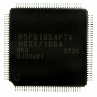
DF61654N50FTV Renesas Electronics America, DF61654N50FTV Datasheet - Page 759

DF61654N50FTV
Manufacturer Part Number
DF61654N50FTV
Description
IC H8SX/1654 MCU FLASH 120TQFP
Manufacturer
Renesas Electronics America
Series
H8® H8SX/1600r
Datasheet
1.DF61653N50FTV.pdf
(1020 pages)
Specifications of DF61654N50FTV
Core Processor
H8SX
Core Size
32-Bit
Speed
50MHz
Connectivity
I²C, IrDA, SCI, SmartCard, USB
Peripherals
DMA, PWM, WDT
Number Of I /o
75
Program Memory Size
512KB (512K x 8)
Program Memory Type
FLASH
Ram Size
40K x 8
Voltage - Supply (vcc/vdd)
3 V ~ 3.6 V
Data Converters
A/D 8x10b; D/A 2x8b
Oscillator Type
External
Operating Temperature
-20°C ~ 75°C
Package / Case
120-TQFP, 120-VQFP
For Use With
HS0005KCU11H - EMULATOR E10A-USB H8S(X),SH2(A)3DK1657 - DEV EVAL KIT FOR H8SX/1657
Lead Free Status / RoHS Status
Lead free / RoHS Compliant
Eeprom Size
-
Available stocks
Company
Part Number
Manufacturer
Quantity
Price
Company:
Part Number:
DF61654N50FTV
Manufacturer:
Renesas Electronics America
Quantity:
10 000
- Current page: 759 of 1020
- Download datasheet (6Mb)
Bit
7
6
5
4
3
2
1
0
Bit Name
BBSY
SCP
SDAO
SCLO
IICRST
0
Initial
Value
0
1
1
1
1
1
1
R/W
R/W
R/W
R
R/W
R
R/W
Description
Bus Busy
This bit indicates whether the I
released and to issue start and stop conditions in
master mode. This bit is set to 1 when the SDA level
changes from high to low under the condition of SCL =
high, assuming that the start condition has been
issued. This bit is cleared to 0 when the SDA level
changes from low to high under the condition of SDA =
high, assuming that the stop condition has been
issued. Follow this procedure also when re-transmitting
a start condition. To issue a start or stop condition, use
the MOV instruction.
Start/Stop Condition Issue
This bit controls the issuance of start or stop condition
in master mode.
To issue a start condition, write 1 to BBSY and 0 to
SCP. A re-transmit start condition is issued in the same
way. To issue a stop condition, write 0 to BBSY and 0
to SCP. This bit is always read as 1. If 1 is written, the
data is not stored.
This bit monitors the output level of SDA.
0: When reading, the SDA pin outputs a low level
1: When reading the SDA pin outputs a high level
Reserved
The write value should always be 1.
This bit monitors the SCL output level.
When reading and SCLO is 1, the SCL pin outputs a
high level. When reading and SCLO is 0, the SCL pin
outputs a low level.
Reserved
This bit is always read as 0.
IIC Control Module Reset
This bit reset the IIC control module except the I
registers. If hang-up occurs because of communication
failure during I
Reserved
This bit is always read as 1.
2
C operation, by setting this bit to 1, the
Rev.1.00 Sep. 08, 2005 Page 709 of 966
Section 16 I
2
C bus is occupied or
2
C Bus Interface2 (IIC2)
REJ09B0219-0100
2
C
Related parts for DF61654N50FTV
Image
Part Number
Description
Manufacturer
Datasheet
Request
R

Part Number:
Description:
KIT STARTER FOR M16C/29
Manufacturer:
Renesas Electronics America
Datasheet:

Part Number:
Description:
KIT STARTER FOR R8C/2D
Manufacturer:
Renesas Electronics America
Datasheet:

Part Number:
Description:
R0K33062P STARTER KIT
Manufacturer:
Renesas Electronics America
Datasheet:

Part Number:
Description:
KIT STARTER FOR R8C/23 E8A
Manufacturer:
Renesas Electronics America
Datasheet:

Part Number:
Description:
KIT STARTER FOR R8C/25
Manufacturer:
Renesas Electronics America
Datasheet:

Part Number:
Description:
KIT STARTER H8S2456 SHARPE DSPLY
Manufacturer:
Renesas Electronics America
Datasheet:

Part Number:
Description:
KIT STARTER FOR R8C38C
Manufacturer:
Renesas Electronics America
Datasheet:

Part Number:
Description:
KIT STARTER FOR R8C35C
Manufacturer:
Renesas Electronics America
Datasheet:

Part Number:
Description:
KIT STARTER FOR R8CL3AC+LCD APPS
Manufacturer:
Renesas Electronics America
Datasheet:

Part Number:
Description:
KIT STARTER FOR RX610
Manufacturer:
Renesas Electronics America
Datasheet:

Part Number:
Description:
KIT STARTER FOR R32C/118
Manufacturer:
Renesas Electronics America
Datasheet:

Part Number:
Description:
KIT DEV RSK-R8C/26-29
Manufacturer:
Renesas Electronics America
Datasheet:

Part Number:
Description:
KIT STARTER FOR SH7124
Manufacturer:
Renesas Electronics America
Datasheet:

Part Number:
Description:
KIT STARTER FOR H8SX/1622
Manufacturer:
Renesas Electronics America
Datasheet:

Part Number:
Description:
KIT DEV FOR SH7203
Manufacturer:
Renesas Electronics America
Datasheet:


