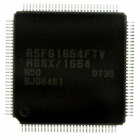
DF61654N50FTV Renesas Electronics America, DF61654N50FTV Datasheet - Page 850

DF61654N50FTV
Manufacturer Part Number
DF61654N50FTV
Description
IC H8SX/1654 MCU FLASH 120TQFP
Manufacturer
Renesas Electronics America
Series
H8® H8SX/1600r
Datasheet
1.DF61653N50FTV.pdf
(1020 pages)
Specifications of DF61654N50FTV
Core Processor
H8SX
Core Size
32-Bit
Speed
50MHz
Connectivity
I²C, IrDA, SCI, SmartCard, USB
Peripherals
DMA, PWM, WDT
Number Of I /o
75
Program Memory Size
512KB (512K x 8)
Program Memory Type
FLASH
Ram Size
40K x 8
Voltage - Supply (vcc/vdd)
3 V ~ 3.6 V
Data Converters
A/D 8x10b; D/A 2x8b
Oscillator Type
External
Operating Temperature
-20°C ~ 75°C
Package / Case
120-TQFP, 120-VQFP
For Use With
HS0005KCU11H - EMULATOR E10A-USB H8S(X),SH2(A)3DK1657 - DEV EVAL KIT FOR H8SX/1657
Lead Free Status / RoHS Status
Lead free / RoHS Compliant
Eeprom Size
-
Available stocks
Company
Part Number
Manufacturer
Quantity
Price
Company:
Part Number:
DF61654N50FTV
Manufacturer:
Renesas Electronics America
Quantity:
10 000
- Current page: 850 of 1020
- Download datasheet (6Mb)
Section 20 Flash Memory (0.18-µm F-ZTAT Version)
The procedure program must be executed in an area other than the flash memory to be
programmed. Setting the SCO bit in FCCS to 1 to request download must be executed in the on-
chip RAM. The area that can be executed in the steps of the procedure program (on-chip RAM,
user MAT, and external space) is shown in section 20.7.4, On-Chip Program and Storable Area for
Program Data. The following description assumes that the area to be programmed on the user
MAT is erased and that program data is prepared in the consecutive area.
The program data for one programming operation is always 128 bytes. When the program data
exceeds 128 bytes, the start address of the programming destination and program data parameters
are updated in 128-byte units and programming is repeated. When the program data is less than
128 bytes, invalid data is filled to prepare 128-byte program data. If the invalid data to be added is
H'FF, the program processing time can be shortened.
1. Select the on-chip program to be downloaded and the download destination. When the PPVS
2. Write H'A5 in FKEY. If H'A5 is not written to FKEY, the SCO bit in FCCS cannot be set to 1
3. After initializing VBR to H'00000000, set the SCO bit to 1 to execute download. To set the
Rev.1.00 Sep. 08, 2005 Page 800 of 966
REJ09B0219-0100
bit in FPCS is set to 1, the programming program is selected. Several programming/erasing
programs cannot be selected at one time. If several programs are selected, a download error is
returned to the SS bit in the DPFR parameter. The on-chip RAM start address of the download
destination is specified by FTDAR.
to request download of the on-chip program.
SCO bit to 1, all of the following conditions must be satisfied.
RAM emulation mode has been canceled.
H'A5 is written to FKEY.
Setting the SCO bit is executed in the on-chip RAM.
When the SCO bit is set to 1, download is started automatically. Since the SCO bit is cleared
to 0 when the procedure program is resumed, the SCO bit cannot be confirmed to be 1 in the
procedure program. The download result can be confirmed by the return value of the DPFR
parameter. To prevent incorrect decision, before setting the SCO bit to 1, set one byte of the
on-chip RAM start address specified by FTDAR, which becomes the DPFR parameter, to a
value other than the return value (e.g. H'FF). Since particular processing that is accompanied
by bank switching as described below is performed when download is executed, initialize the
VBR contents to H'00000000. Dummy read of FCCS must be performed twice immediately
after the SCO bit is set to 1.
The user-MAT space is switched to the on-chip program storage area.
After the program to be downloaded and the on-chip RAM start address specified by
FPCS, FECS, and the SCO bit in FCCS are cleared to 0.
FTDAR are checked, they are transferred to the on-chip RAM.
Related parts for DF61654N50FTV
Image
Part Number
Description
Manufacturer
Datasheet
Request
R

Part Number:
Description:
KIT STARTER FOR M16C/29
Manufacturer:
Renesas Electronics America
Datasheet:

Part Number:
Description:
KIT STARTER FOR R8C/2D
Manufacturer:
Renesas Electronics America
Datasheet:

Part Number:
Description:
R0K33062P STARTER KIT
Manufacturer:
Renesas Electronics America
Datasheet:

Part Number:
Description:
KIT STARTER FOR R8C/23 E8A
Manufacturer:
Renesas Electronics America
Datasheet:

Part Number:
Description:
KIT STARTER FOR R8C/25
Manufacturer:
Renesas Electronics America
Datasheet:

Part Number:
Description:
KIT STARTER H8S2456 SHARPE DSPLY
Manufacturer:
Renesas Electronics America
Datasheet:

Part Number:
Description:
KIT STARTER FOR R8C38C
Manufacturer:
Renesas Electronics America
Datasheet:

Part Number:
Description:
KIT STARTER FOR R8C35C
Manufacturer:
Renesas Electronics America
Datasheet:

Part Number:
Description:
KIT STARTER FOR R8CL3AC+LCD APPS
Manufacturer:
Renesas Electronics America
Datasheet:

Part Number:
Description:
KIT STARTER FOR RX610
Manufacturer:
Renesas Electronics America
Datasheet:

Part Number:
Description:
KIT STARTER FOR R32C/118
Manufacturer:
Renesas Electronics America
Datasheet:

Part Number:
Description:
KIT DEV RSK-R8C/26-29
Manufacturer:
Renesas Electronics America
Datasheet:

Part Number:
Description:
KIT STARTER FOR SH7124
Manufacturer:
Renesas Electronics America
Datasheet:

Part Number:
Description:
KIT STARTER FOR H8SX/1622
Manufacturer:
Renesas Electronics America
Datasheet:

Part Number:
Description:
KIT DEV FOR SH7203
Manufacturer:
Renesas Electronics America
Datasheet:


