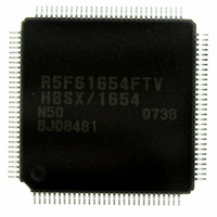
DF61654N50FTV Renesas Electronics America, DF61654N50FTV Datasheet - Page 660

DF61654N50FTV
Manufacturer Part Number
DF61654N50FTV
Description
IC H8SX/1654 MCU FLASH 120TQFP
Manufacturer
Renesas Electronics America
Series
H8® H8SX/1600r
Datasheet
1.DF61653N50FTV.pdf
(1020 pages)
Specifications of DF61654N50FTV
Core Processor
H8SX
Core Size
32-Bit
Speed
50MHz
Connectivity
I²C, IrDA, SCI, SmartCard, USB
Peripherals
DMA, PWM, WDT
Number Of I /o
75
Program Memory Size
512KB (512K x 8)
Program Memory Type
FLASH
Ram Size
40K x 8
Voltage - Supply (vcc/vdd)
3 V ~ 3.6 V
Data Converters
A/D 8x10b; D/A 2x8b
Oscillator Type
External
Operating Temperature
-20°C ~ 75°C
Package / Case
120-TQFP, 120-VQFP
For Use With
HS0005KCU11H - EMULATOR E10A-USB H8S(X),SH2(A)3DK1657 - DEV EVAL KIT FOR H8SX/1657
Lead Free Status / RoHS Status
Lead free / RoHS Compliant
Eeprom Size
-
Available stocks
Company
Part Number
Manufacturer
Quantity
Price
Company:
Part Number:
DF61654N50FTV
Manufacturer:
Renesas Electronics America
Quantity:
10 000
- Current page: 660 of 1020
- Download datasheet (6Mb)
Section 14 Serial Communication Interface (SCI, IrDA, CRC)
14.7
The SCI supports the smart card interface, supporting the ISO/IEC 7816-3 (Identification Card)
standard, as an extended serial communication interface function. Smart card interface mode can
be selected using the appropriate register.
14.7.1
Figure 14.24 shows a sample connection between the smart card and this LSI. As in the figure,
since this LSI communicates with the smart card using a single transmission line, interconnect the
TxD and RxD pins and pull up the data transmission line to V
and TE bits to 1 with the smart card not connected enables closed transmission/reception allowing
self diagnosis. To supply the smart card with the clock pulses generated by the SCI, input the SCK
pin output to the CLK pin of the smart card. A reset signal can be supplied via the output port of
this LSI. (In SCI_5 and SCI-6, the clock generated in SCI cannot be provided to smart cards.)
Rev.1.00 Sep. 08, 2005 Page 610 of 966
REJ09B0219-0100
Operation in Smart Card Interface Mode
Sample Connection
Figure 14.24 Pin Connection for Smart Card Interface
Main unit of the device
to be connected
This LSI
Rx (port)
SCK
RxD
TxD
Reset line
Clock line
Data line
V
CC
CC
I/O
CLK
RST
using a resistor. Setting the RE
Smart card
Related parts for DF61654N50FTV
Image
Part Number
Description
Manufacturer
Datasheet
Request
R

Part Number:
Description:
KIT STARTER FOR M16C/29
Manufacturer:
Renesas Electronics America
Datasheet:

Part Number:
Description:
KIT STARTER FOR R8C/2D
Manufacturer:
Renesas Electronics America
Datasheet:

Part Number:
Description:
R0K33062P STARTER KIT
Manufacturer:
Renesas Electronics America
Datasheet:

Part Number:
Description:
KIT STARTER FOR R8C/23 E8A
Manufacturer:
Renesas Electronics America
Datasheet:

Part Number:
Description:
KIT STARTER FOR R8C/25
Manufacturer:
Renesas Electronics America
Datasheet:

Part Number:
Description:
KIT STARTER H8S2456 SHARPE DSPLY
Manufacturer:
Renesas Electronics America
Datasheet:

Part Number:
Description:
KIT STARTER FOR R8C38C
Manufacturer:
Renesas Electronics America
Datasheet:

Part Number:
Description:
KIT STARTER FOR R8C35C
Manufacturer:
Renesas Electronics America
Datasheet:

Part Number:
Description:
KIT STARTER FOR R8CL3AC+LCD APPS
Manufacturer:
Renesas Electronics America
Datasheet:

Part Number:
Description:
KIT STARTER FOR RX610
Manufacturer:
Renesas Electronics America
Datasheet:

Part Number:
Description:
KIT STARTER FOR R32C/118
Manufacturer:
Renesas Electronics America
Datasheet:

Part Number:
Description:
KIT DEV RSK-R8C/26-29
Manufacturer:
Renesas Electronics America
Datasheet:

Part Number:
Description:
KIT STARTER FOR SH7124
Manufacturer:
Renesas Electronics America
Datasheet:

Part Number:
Description:
KIT STARTER FOR H8SX/1622
Manufacturer:
Renesas Electronics America
Datasheet:

Part Number:
Description:
KIT DEV FOR SH7203
Manufacturer:
Renesas Electronics America
Datasheet:


