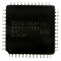
DF61654N50FTV Renesas Electronics America, DF61654N50FTV Datasheet - Page 661

DF61654N50FTV
Manufacturer Part Number
DF61654N50FTV
Description
IC H8SX/1654 MCU FLASH 120TQFP
Manufacturer
Renesas Electronics America
Series
H8® H8SX/1600r
Datasheet
1.DF61653N50FTV.pdf
(1020 pages)
Specifications of DF61654N50FTV
Core Processor
H8SX
Core Size
32-Bit
Speed
50MHz
Connectivity
I²C, IrDA, SCI, SmartCard, USB
Peripherals
DMA, PWM, WDT
Number Of I /o
75
Program Memory Size
512KB (512K x 8)
Program Memory Type
FLASH
Ram Size
40K x 8
Voltage - Supply (vcc/vdd)
3 V ~ 3.6 V
Data Converters
A/D 8x10b; D/A 2x8b
Oscillator Type
External
Operating Temperature
-20°C ~ 75°C
Package / Case
120-TQFP, 120-VQFP
For Use With
HS0005KCU11H - EMULATOR E10A-USB H8S(X),SH2(A)3DK1657 - DEV EVAL KIT FOR H8SX/1657
Lead Free Status / RoHS Status
Lead free / RoHS Compliant
Eeprom Size
-
Available stocks
Company
Part Number
Manufacturer
Quantity
Price
Company:
Part Number:
DF61654N50FTV
Manufacturer:
Renesas Electronics America
Quantity:
10 000
- Current page: 661 of 1020
- Download datasheet (6Mb)
14.7.2
Figure 14.25 shows the data transfer formats in smart card interface mode.
• One frame contains 8-bit data and a parity bit in asynchronous mode.
• During transmission, at least 2 etu (elementary time unit: time required for transferring one bit)
• If a parity error is detected during reception, a low error signal is output for 1 etu after 10.5 etu
• If an error signal is sampled during transmission, the same data is automatically re-transmitted
For communication with the smart cards of the direct convention and inverse convention types,
follow the procedure below.
is secured as a guard time after the end of the parity bit before the start of the next frame.
has passed from the start bit.
after at least 2 etu.
In normal transmission/reception
When a parity error is generated
[Legend]
Ds:
D0 to D7: Data bits
Dp:
DE:
Data Format (Except in Block Transfer Mode)
Figure 14.25 Data Formats in Normal Smart Card Interface Mode
(Z)
Ds
Ds
Start bit
Parity bit
Error signal
Figure 14.26 Direct Convention (SDIR = SINV = O/E = 0)
Ds
A
D0
D0
D0
Z
D1
D1
D1
Z
Output from the transmitting station
Output from the transmitting station
D2
D2
D2
A
D3
D3
D3
Z
Section 14 Serial Communication Interface (SCI, IrDA, CRC)
D4
Z
D4
D4
D5
Z
D5
D5
D6
A
D6
D6
D7
A
Rev.1.00 Sep. 08, 2005 Page 611 of 966
Dp
D7
D7
Z
Dp
Dp
(Z) state
Output from
the receiving station
DE
REJ09B0219-0100
Related parts for DF61654N50FTV
Image
Part Number
Description
Manufacturer
Datasheet
Request
R

Part Number:
Description:
KIT STARTER FOR M16C/29
Manufacturer:
Renesas Electronics America
Datasheet:

Part Number:
Description:
KIT STARTER FOR R8C/2D
Manufacturer:
Renesas Electronics America
Datasheet:

Part Number:
Description:
R0K33062P STARTER KIT
Manufacturer:
Renesas Electronics America
Datasheet:

Part Number:
Description:
KIT STARTER FOR R8C/23 E8A
Manufacturer:
Renesas Electronics America
Datasheet:

Part Number:
Description:
KIT STARTER FOR R8C/25
Manufacturer:
Renesas Electronics America
Datasheet:

Part Number:
Description:
KIT STARTER H8S2456 SHARPE DSPLY
Manufacturer:
Renesas Electronics America
Datasheet:

Part Number:
Description:
KIT STARTER FOR R8C38C
Manufacturer:
Renesas Electronics America
Datasheet:

Part Number:
Description:
KIT STARTER FOR R8C35C
Manufacturer:
Renesas Electronics America
Datasheet:

Part Number:
Description:
KIT STARTER FOR R8CL3AC+LCD APPS
Manufacturer:
Renesas Electronics America
Datasheet:

Part Number:
Description:
KIT STARTER FOR RX610
Manufacturer:
Renesas Electronics America
Datasheet:

Part Number:
Description:
KIT STARTER FOR R32C/118
Manufacturer:
Renesas Electronics America
Datasheet:

Part Number:
Description:
KIT DEV RSK-R8C/26-29
Manufacturer:
Renesas Electronics America
Datasheet:

Part Number:
Description:
KIT STARTER FOR SH7124
Manufacturer:
Renesas Electronics America
Datasheet:

Part Number:
Description:
KIT STARTER FOR H8SX/1622
Manufacturer:
Renesas Electronics America
Datasheet:

Part Number:
Description:
KIT DEV FOR SH7203
Manufacturer:
Renesas Electronics America
Datasheet:


