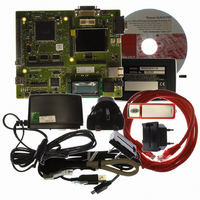
R0K572030S000BE Renesas Electronics America, R0K572030S000BE Datasheet - Page 1087

R0K572030S000BE
Manufacturer Part Number
R0K572030S000BE
Description
KIT DEV FOR SH7203
Manufacturer
Renesas Electronics America
Series
Renesas Starter Kits (RSK)r
Type
MCUr
Specifications of R0K572030S000BE
Contents
CPU Board, LCD Module, E10A-Lite Emulator, Cable, QuickStart Guide and CD-ROM
Silicon Manufacturer
Renesas
Kit Contents
Board
Silicon Family Name
SH7203
Silicon Core Number
R5S72030W200FP
Tool / Board Applications
General Purpose MCU, MPU, DSP, DSC
Mcu Supported Families
SH7203
Lead Free Status / RoHS Status
Contains lead / RoHS non-compliant
For Use With/related Products
SH7203
Lead Free Status / Rohs Status
Compliant
- Current page: 1087 of 1686
- Download datasheet (10Mb)
(7)
• The 224-byte data FIFO register (FLDTFIFO) is incorporated for data transfer of flash
• The 32-byte control code FIFO register (FLECFIFO) is incorporated for data transfer of
(8)
• By individually specifying the destinations of data and control code of flash memory to the
(9)
• The operating clock (FCLK) on the pins for the AND-/NAND-type flash memory is generated
• The division ratio can be specified by the FCKSEL bit and the QTSEL bit in the common
• Before changing the CPG specification, the FLCTL must be placed in a module stop state.
• In NAND-type flash memory, the FSC and FWE pins operate with the FCLK frequency. In
memory.
control code.
DMA controller, data and control code can be sent to different areas.
by dividing the peripheral clock (Pφ).
control register (FLCMNCR).
AND-type flash memory, the FSC pin operates with the FCLK operating frequency and the
FWE pin operates with a frequency half the FCLK operating frequency. The operating
frequencies must be specified within the maximum operating frequency of memory to be
connected.
Data Transfer FIFO and Data Register
DMA Transfer
Access Time
Section 22 AND/NAND Flash Memory Controller (FLCTL)
Rev. 3.00 Sep. 28, 2009 Page 1055 of 1650
REJ09B0313-0300
Related parts for R0K572030S000BE
Image
Part Number
Description
Manufacturer
Datasheet
Request
R

Part Number:
Description:
KIT STARTER FOR M16C/29
Manufacturer:
Renesas Electronics America
Datasheet:

Part Number:
Description:
KIT STARTER FOR R8C/2D
Manufacturer:
Renesas Electronics America
Datasheet:

Part Number:
Description:
R0K33062P STARTER KIT
Manufacturer:
Renesas Electronics America
Datasheet:

Part Number:
Description:
KIT STARTER FOR R8C/23 E8A
Manufacturer:
Renesas Electronics America
Datasheet:

Part Number:
Description:
KIT STARTER FOR R8C/25
Manufacturer:
Renesas Electronics America
Datasheet:

Part Number:
Description:
KIT STARTER H8S2456 SHARPE DSPLY
Manufacturer:
Renesas Electronics America
Datasheet:

Part Number:
Description:
KIT STARTER FOR R8C38C
Manufacturer:
Renesas Electronics America
Datasheet:

Part Number:
Description:
KIT STARTER FOR R8C35C
Manufacturer:
Renesas Electronics America
Datasheet:

Part Number:
Description:
KIT STARTER FOR R8CL3AC+LCD APPS
Manufacturer:
Renesas Electronics America
Datasheet:

Part Number:
Description:
KIT STARTER FOR RX610
Manufacturer:
Renesas Electronics America
Datasheet:

Part Number:
Description:
KIT STARTER FOR R32C/118
Manufacturer:
Renesas Electronics America
Datasheet:

Part Number:
Description:
KIT DEV RSK-R8C/26-29
Manufacturer:
Renesas Electronics America
Datasheet:

Part Number:
Description:
KIT STARTER FOR SH7124
Manufacturer:
Renesas Electronics America
Datasheet:

Part Number:
Description:
KIT STARTER FOR H8SX/1622
Manufacturer:
Renesas Electronics America
Datasheet:

Part Number:
Description:
KIT STARTER FOR R8C/18191A1B
Manufacturer:
Renesas Electronics America
Datasheet:


