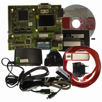
R0K572030S000BE Renesas Electronics America, R0K572030S000BE Datasheet - Page 413

R0K572030S000BE
Manufacturer Part Number
R0K572030S000BE
Description
KIT DEV FOR SH7203
Manufacturer
Renesas Electronics America
Series
Renesas Starter Kits (RSK)r
Type
MCUr
Specifications of R0K572030S000BE
Contents
CPU Board, LCD Module, E10A-Lite Emulator, Cable, QuickStart Guide and CD-ROM
Silicon Manufacturer
Renesas
Kit Contents
Board
Silicon Family Name
SH7203
Silicon Core Number
R5S72030W200FP
Tool / Board Applications
General Purpose MCU, MPU, DSP, DSC
Mcu Supported Families
SH7203
Lead Free Status / RoHS Status
Contains lead / RoHS non-compliant
For Use With/related Products
SH7203
Lead Free Status / Rohs Status
Compliant
- Current page: 413 of 1686
- Download datasheet (10Mb)
Table 9.21 Conditions for Determining Number of Idle Cycles
No. Condition
[1]
[2]
[3]
[4]
DMAIW[2:0] in
CMNCR
IW***[2:0] in
CSnBCR
SDRAM-related
bits in
CSnWCR
WM in
CSnWCR
Description
These bits specify the number of
idle cycles for DMA single address
transfer. This condition is effective
only for single address transfer and
generates idle cycles after the
access is completed.
These bits specify the number of
idle cycles for access other than
single address transfer. The
number of idle cycles can be
specified independently for each
combination of the previous and
next cycles. For example, in the
case where reading CS1 space
followed by reading other CS
space, the bits IWRRD[2:0] in
CS1BCR should be set to B'100 to
specify six or more idle cycles. This
condition is effective only for access
cycles other than single address
transfer and generates idle cycles
after the access is completed.
These bits specify precharge
completion and startup wait cycles
and idle cycles between commands
for SDRAM access. This condition
is effective only for SDRAM access
and generates idle cycles after the
access is completed
This bit enables or disables external
WAIT pin input for the memory
types other than SDRAM. When
this bit is cleared to 0 (external
WAIT enabled), one idle cycle is
inserted to check the external WAIT
pin input after the access is
completed. When this bit is set to 1
(disabled), no idle cycle is
generated.
Range Note
0 to 12 When 0 is specified for the
0 to 12 Do not set 0 for the number of
0 to 3
0 or 1
Rev. 3.00 Sep. 28, 2009 Page 381 of 1650
Section 9 Bus State Controller (BSC)
number of idle cycles, the
DACK signal may be asserted
continuously. This causes a
discrepancy between the
number of cycles detected by
the device with DACK and the
DMAC transfer count, resulting
in a malfunction.
idle cycles between memory
types which are not allowed to
be accessed successively.
accordance with the
specification of the target
SDRAM.
Specify these bits in
REJ09B0313-0300
Related parts for R0K572030S000BE
Image
Part Number
Description
Manufacturer
Datasheet
Request
R

Part Number:
Description:
KIT STARTER FOR M16C/29
Manufacturer:
Renesas Electronics America
Datasheet:

Part Number:
Description:
KIT STARTER FOR R8C/2D
Manufacturer:
Renesas Electronics America
Datasheet:

Part Number:
Description:
R0K33062P STARTER KIT
Manufacturer:
Renesas Electronics America
Datasheet:

Part Number:
Description:
KIT STARTER FOR R8C/23 E8A
Manufacturer:
Renesas Electronics America
Datasheet:

Part Number:
Description:
KIT STARTER FOR R8C/25
Manufacturer:
Renesas Electronics America
Datasheet:

Part Number:
Description:
KIT STARTER H8S2456 SHARPE DSPLY
Manufacturer:
Renesas Electronics America
Datasheet:

Part Number:
Description:
KIT STARTER FOR R8C38C
Manufacturer:
Renesas Electronics America
Datasheet:

Part Number:
Description:
KIT STARTER FOR R8C35C
Manufacturer:
Renesas Electronics America
Datasheet:

Part Number:
Description:
KIT STARTER FOR R8CL3AC+LCD APPS
Manufacturer:
Renesas Electronics America
Datasheet:

Part Number:
Description:
KIT STARTER FOR RX610
Manufacturer:
Renesas Electronics America
Datasheet:

Part Number:
Description:
KIT STARTER FOR R32C/118
Manufacturer:
Renesas Electronics America
Datasheet:

Part Number:
Description:
KIT DEV RSK-R8C/26-29
Manufacturer:
Renesas Electronics America
Datasheet:

Part Number:
Description:
KIT STARTER FOR SH7124
Manufacturer:
Renesas Electronics America
Datasheet:

Part Number:
Description:
KIT STARTER FOR H8SX/1622
Manufacturer:
Renesas Electronics America
Datasheet:

Part Number:
Description:
KIT STARTER FOR R8C/18191A1B
Manufacturer:
Renesas Electronics America
Datasheet:


