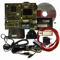
R0K572030S000BE Renesas Electronics America, R0K572030S000BE Datasheet - Page 214

R0K572030S000BE
Manufacturer Part Number
R0K572030S000BE
Description
KIT DEV FOR SH7203
Manufacturer
Renesas Electronics America
Series
Renesas Starter Kits (RSK)r
Type
MCUr
Specifications of R0K572030S000BE
Contents
CPU Board, LCD Module, E10A-Lite Emulator, Cable, QuickStart Guide and CD-ROM
Silicon Manufacturer
Renesas
Kit Contents
Board
Silicon Family Name
SH7203
Silicon Core Number
R5S72030W200FP
Tool / Board Applications
General Purpose MCU, MPU, DSP, DSC
Mcu Supported Families
SH7203
Lead Free Status / RoHS Status
Contains lead / RoHS non-compliant
For Use With/related Products
SH7203
Lead Free Status / Rohs Status
Compliant
- Current page: 214 of 1686
- Download datasheet (10Mb)
Section 6 Interrupt Controller (INTC)
6.7
Table 6.5 lists the interrupt response time, which is the time from the occurrence of an interrupt
request until the interrupt exception handling starts and fetching of the first instruction in the
exception service routine begins. The interrupt processing operations differ in the cases when
banking is disabled, when banking is enabled without register bank overflow, and when banking is
enabled with register bank overflow. Figures 6.4 and 6.5 show examples of pipeline operation
when banking is disabled. Figures 6.6 and 6.7 show examples of pipeline operation when banking
is enabled without register bank overflow. Figures 6.8 and 6.9 show examples of pipeline
operation when banking is enabled with register bank overflow.
Table 6.5
Rev. 3.00 Sep. 28, 2009 Page 182 of 1650
REJ09B0313-0300
Item
Time from occurrence of interrupt
request until interrupt controller
identifies priority, compares it with
mask bits in SR, and sends interrupt
request signal to CPU
Time from
input of
interrupt
request signal
to CPU until
sequence
currently being
executed is
completed,
interrupt
exception
handling starts,
and first
instruction in
interrupt
exception
service routine
is fetched
Interrupt Response Time
No register
banking
Register
banking
without
register
bank
overflow
Register
banking
with
register
bank
overflow
Interrupt Response Time
Min.
Max.
Min.
Max.
Min.
Max.
NMI
2 Icyc +
2 Bcyc +
1 Pcyc
3 Icyc + m1 + m2
4 Icyc + 2(m1 + m2) + m3
⎯
⎯
⎯
⎯
User
Break
3 Icyc
H-UDI
2 Icyc +
1 Pcyc
3 Icyc + m1 + m2
12 Icyc + m1 + m2
3 Icyc + m1 + m2
3 Icyc + m1 + m2 + 19(m4)
Number of States
IRQ, PINT
2 Icyc +
3 Bcyc +
1 Pcyc
USB
2 Icyc +
4 Bcyc
Peripheral
Module
(Other
than USB) Remarks
2 Icyc +
2 Bcyc
Min. is when the interrupt
wait time is zero.
Max. is when a higher-
priority interrupt request has
occurred during interrupt
exception handling.
Min. is when the interrupt
wait time is zero.
Max. is when an interrupt
request has occurred during
execution of the RESBANK
instruction.
Min. is when the interrupt
wait time is zero.
Max. is when an interrupt
request has occurred during
execution of the RESBANK
instruction.
Related parts for R0K572030S000BE
Image
Part Number
Description
Manufacturer
Datasheet
Request
R

Part Number:
Description:
KIT STARTER FOR M16C/29
Manufacturer:
Renesas Electronics America
Datasheet:

Part Number:
Description:
KIT STARTER FOR R8C/2D
Manufacturer:
Renesas Electronics America
Datasheet:

Part Number:
Description:
R0K33062P STARTER KIT
Manufacturer:
Renesas Electronics America
Datasheet:

Part Number:
Description:
KIT STARTER FOR R8C/23 E8A
Manufacturer:
Renesas Electronics America
Datasheet:

Part Number:
Description:
KIT STARTER FOR R8C/25
Manufacturer:
Renesas Electronics America
Datasheet:

Part Number:
Description:
KIT STARTER H8S2456 SHARPE DSPLY
Manufacturer:
Renesas Electronics America
Datasheet:

Part Number:
Description:
KIT STARTER FOR R8C38C
Manufacturer:
Renesas Electronics America
Datasheet:

Part Number:
Description:
KIT STARTER FOR R8C35C
Manufacturer:
Renesas Electronics America
Datasheet:

Part Number:
Description:
KIT STARTER FOR R8CL3AC+LCD APPS
Manufacturer:
Renesas Electronics America
Datasheet:

Part Number:
Description:
KIT STARTER FOR RX610
Manufacturer:
Renesas Electronics America
Datasheet:

Part Number:
Description:
KIT STARTER FOR R32C/118
Manufacturer:
Renesas Electronics America
Datasheet:

Part Number:
Description:
KIT DEV RSK-R8C/26-29
Manufacturer:
Renesas Electronics America
Datasheet:

Part Number:
Description:
KIT STARTER FOR SH7124
Manufacturer:
Renesas Electronics America
Datasheet:

Part Number:
Description:
KIT STARTER FOR H8SX/1622
Manufacturer:
Renesas Electronics America
Datasheet:

Part Number:
Description:
KIT STARTER FOR R8C/18191A1B
Manufacturer:
Renesas Electronics America
Datasheet:


