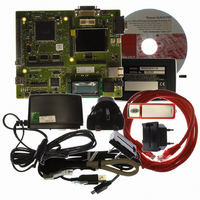
R0K572030S000BE Renesas Electronics America, R0K572030S000BE Datasheet - Page 277

R0K572030S000BE
Manufacturer Part Number
R0K572030S000BE
Description
KIT DEV FOR SH7203
Manufacturer
Renesas Electronics America
Series
Renesas Starter Kits (RSK)r
Type
MCUr
Specifications of R0K572030S000BE
Contents
CPU Board, LCD Module, E10A-Lite Emulator, Cable, QuickStart Guide and CD-ROM
Silicon Manufacturer
Renesas
Kit Contents
Board
Silicon Family Name
SH7203
Silicon Core Number
R5S72030W200FP
Tool / Board Applications
General Purpose MCU, MPU, DSP, DSC
Mcu Supported Families
SH7203
Lead Free Status / RoHS Status
Contains lead / RoHS non-compliant
For Use With/related Products
SH7203
Lead Free Status / Rohs Status
Compliant
- Current page: 277 of 1686
- Download datasheet (10Mb)
Note:
9.3.2
In this LSI, the data bus width of area 0 and the initial data bus width of areas 1 to 7 can be set to
16, or 32 bits through external pins during a power-on reset. The bus width of area 0 cannot be
modified after a power-on reset. The initial data bus width of areas 1 to 7 is set to the same size as
that of area 0, but can be modified to 8, 16, or 32 bits through register settings during program
execution. Note that the selectable data bus widths may be limited depending on the connected
memory type.
After a power-on reset, the LSI starts execution of the program stored in the external memory
allocated in area 0. Since ROM is assumed as the external memory in area 0, minimum pin
functions such as the address bus, data bus, CS0, and RD are available. The sample access
waveforms shown in this section include other pins such as BS, RD/WR, and WEn, which are
available after they are selected through the pin function controller. Do not attempt any form of
memory access other than reading of area 0 until the pin function settings have been completed by
the program. When the LSI has been started up with a 32-bit bus and the bus width of an area
other than area 0 is changed to 16 bits, the A1 pin setting becomes necessary for access to that
area. In the same way, both A1 and A0 pin settings become necessary when the bus width of an
area is changed to 8 bits. When area 7 is in use, the CS7 and A0 functions are assigned to the same
pin. In this case, therefore, note that the 8-bit bus width is not selectable.
For details on pin function settings, see section 25, Pin Function Controller (PFC).
Table 9.3
Internal Address
H'80000000 to H'FFFBFFFF Other
H'FFFC0000 to H'FFFFFFFF Other
MD
1
0
* For the on-chip RAM space, access the addresses shown in section 27, On-Chip RAM.
Data Bus Width and Pin Function Setting in Each Area
For the on-chip peripheral module space, access the addresses shown in section 30,
List of Registers. Do not access addresses which are not described in these sections.
Otherwise, the correct operation cannot be guaranteed.
Correspondence between External Pin (MD) and Data Bus Width
Space Memory to be Connected
On-chip RAM, reserved area*
On-chip peripheral modules, reserved area*
Data Bus Width
32 bits
16 bits
Rev. 3.00 Sep. 28, 2009 Page 245 of 1650
Section 9 Bus State Controller (BSC)
Cache
⎯
⎯
REJ09B0313-0300
Related parts for R0K572030S000BE
Image
Part Number
Description
Manufacturer
Datasheet
Request
R

Part Number:
Description:
KIT STARTER FOR M16C/29
Manufacturer:
Renesas Electronics America
Datasheet:

Part Number:
Description:
KIT STARTER FOR R8C/2D
Manufacturer:
Renesas Electronics America
Datasheet:

Part Number:
Description:
R0K33062P STARTER KIT
Manufacturer:
Renesas Electronics America
Datasheet:

Part Number:
Description:
KIT STARTER FOR R8C/23 E8A
Manufacturer:
Renesas Electronics America
Datasheet:

Part Number:
Description:
KIT STARTER FOR R8C/25
Manufacturer:
Renesas Electronics America
Datasheet:

Part Number:
Description:
KIT STARTER H8S2456 SHARPE DSPLY
Manufacturer:
Renesas Electronics America
Datasheet:

Part Number:
Description:
KIT STARTER FOR R8C38C
Manufacturer:
Renesas Electronics America
Datasheet:

Part Number:
Description:
KIT STARTER FOR R8C35C
Manufacturer:
Renesas Electronics America
Datasheet:

Part Number:
Description:
KIT STARTER FOR R8CL3AC+LCD APPS
Manufacturer:
Renesas Electronics America
Datasheet:

Part Number:
Description:
KIT STARTER FOR RX610
Manufacturer:
Renesas Electronics America
Datasheet:

Part Number:
Description:
KIT STARTER FOR R32C/118
Manufacturer:
Renesas Electronics America
Datasheet:

Part Number:
Description:
KIT DEV RSK-R8C/26-29
Manufacturer:
Renesas Electronics America
Datasheet:

Part Number:
Description:
KIT STARTER FOR SH7124
Manufacturer:
Renesas Electronics America
Datasheet:

Part Number:
Description:
KIT STARTER FOR H8SX/1622
Manufacturer:
Renesas Electronics America
Datasheet:

Part Number:
Description:
KIT STARTER FOR R8C/18191A1B
Manufacturer:
Renesas Electronics America
Datasheet:


