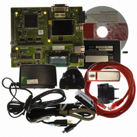
R0K572030S000BE Renesas Electronics America, R0K572030S000BE Datasheet - Page 266

R0K572030S000BE
Manufacturer Part Number
R0K572030S000BE
Description
KIT DEV FOR SH7203
Manufacturer
Renesas Electronics America
Series
Renesas Starter Kits (RSK)r
Type
MCUr
Specifications of R0K572030S000BE
Contents
CPU Board, LCD Module, E10A-Lite Emulator, Cable, QuickStart Guide and CD-ROM
Silicon Manufacturer
Renesas
Kit Contents
Board
Silicon Family Name
SH7203
Silicon Core Number
R5S72030W200FP
Tool / Board Applications
General Purpose MCU, MPU, DSP, DSC
Mcu Supported Families
SH7203
Lead Free Status / RoHS Status
Contains lead / RoHS non-compliant
For Use With/related Products
SH7203
Lead Free Status / Rohs Status
Compliant
- Current page: 266 of 1686
- Download datasheet (10Mb)
Section 8 Cache
8.4
To allow software management of the cache, cache contents can be read and written by means of
MOV instructions. The instruction cache address array is mapped onto addresses H'F000 0000 to
H'F07F FFFF, and the data array onto addresses H'F100 0000 to H'F17F FFFF. The operand cache
address array is mapped onto addresses H'F080 0000 to H'F0FF FFFF, and the data array onto
addresses H'F180 0000 to H'F1FF FFFF. Only longword can be used as the access size for the
address array and data array, and instruction fetches cannot be performed.
8.4.1
To access an address array, the 32-bit address field (for read/write accesses) and 32-bit data field
(for write accesses) must be specified.
In the address field, specify the entry address selecting the entry, The W bit for selecting the way,
and the A bit for specifying the existence of associative operation. In the W bit, B'00 is way 0,
B'01 is way 1, B'10 is way 2, and B'11 is way 3. Since the access size of the address array is fixed
at longword, specify B'00 for bits 1 and 0 of the address.
The tag address, LRU bits, U bit (only for operand cache), and V bit are specified as data. Always
specify 0 for the upper three bits (bits 31 to 29) of the tag address.
For the address and data formats, see figure 8.4.
The following three operations are possible for the address array.
(1)
The tag address, LRU bits, U bit (only for operand cache), and V bit are read from the entry
address specified by the address and the entry corresponding to the way. For the read operation,
associative operation is not performed regardless of whether the associative bit (A bit) specified
by the address is 1 or 0.
(2)
When the associative bit (A bit) in the address field is cleared to 0, write the tag address, LRU
bits, U bit (only for operand cache), and V bit, specified by the data field, to the entry address
specified by the address and the entry corresponding to the way. When writing to a cache line for
which the U bit = 1 and the V bit =1 in the operand cache address array, write the contents of the
cache line back to memory, then write the tag address, LRU bits, U bit, and V bit specified by the
data field. When 0 is written to the V bit, 0 must also be written to the U bit of that entry. When
Rev. 3.00 Sep. 28, 2009 Page 234 of 1650
REJ09B0313-0300
Address Array Read
Address-Array Write (Non-Associative Operation)
Memory-Mapped Cache
Address Array
Related parts for R0K572030S000BE
Image
Part Number
Description
Manufacturer
Datasheet
Request
R

Part Number:
Description:
KIT STARTER FOR M16C/29
Manufacturer:
Renesas Electronics America
Datasheet:

Part Number:
Description:
KIT STARTER FOR R8C/2D
Manufacturer:
Renesas Electronics America
Datasheet:

Part Number:
Description:
R0K33062P STARTER KIT
Manufacturer:
Renesas Electronics America
Datasheet:

Part Number:
Description:
KIT STARTER FOR R8C/23 E8A
Manufacturer:
Renesas Electronics America
Datasheet:

Part Number:
Description:
KIT STARTER FOR R8C/25
Manufacturer:
Renesas Electronics America
Datasheet:

Part Number:
Description:
KIT STARTER H8S2456 SHARPE DSPLY
Manufacturer:
Renesas Electronics America
Datasheet:

Part Number:
Description:
KIT STARTER FOR R8C38C
Manufacturer:
Renesas Electronics America
Datasheet:

Part Number:
Description:
KIT STARTER FOR R8C35C
Manufacturer:
Renesas Electronics America
Datasheet:

Part Number:
Description:
KIT STARTER FOR R8CL3AC+LCD APPS
Manufacturer:
Renesas Electronics America
Datasheet:

Part Number:
Description:
KIT STARTER FOR RX610
Manufacturer:
Renesas Electronics America
Datasheet:

Part Number:
Description:
KIT STARTER FOR R32C/118
Manufacturer:
Renesas Electronics America
Datasheet:

Part Number:
Description:
KIT DEV RSK-R8C/26-29
Manufacturer:
Renesas Electronics America
Datasheet:

Part Number:
Description:
KIT STARTER FOR SH7124
Manufacturer:
Renesas Electronics America
Datasheet:

Part Number:
Description:
KIT STARTER FOR H8SX/1622
Manufacturer:
Renesas Electronics America
Datasheet:

Part Number:
Description:
KIT STARTER FOR R8C/18191A1B
Manufacturer:
Renesas Electronics America
Datasheet:


