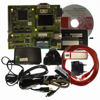
R0K572030S000BE Renesas Electronics America, R0K572030S000BE Datasheet - Page 800

R0K572030S000BE
Manufacturer Part Number
R0K572030S000BE
Description
KIT DEV FOR SH7203
Manufacturer
Renesas Electronics America
Series
Renesas Starter Kits (RSK)r
Type
MCUr
Specifications of R0K572030S000BE
Contents
CPU Board, LCD Module, E10A-Lite Emulator, Cable, QuickStart Guide and CD-ROM
Silicon Manufacturer
Renesas
Kit Contents
Board
Silicon Family Name
SH7203
Silicon Core Number
R5S72030W200FP
Tool / Board Applications
General Purpose MCU, MPU, DSP, DSC
Mcu Supported Families
SH7203
Lead Free Status / RoHS Status
Contains lead / RoHS non-compliant
For Use With/related Products
SH7203
Lead Free Status / Rohs Status
Compliant
- Current page: 800 of 1686
- Download datasheet (10Mb)
Section 15 Serial Communication Interface with FIFO (SCIF)
(2)
An internal clock generated by the on-chip baud rate generator or an external clock input from the
SCK pin can be selected as the SCIF transmit/receive clock. The clock source is selected by the
C/A bit in the serial mode register (SCSMR) and the CKE1 and CKE0 bits in the serial control
register (SCSCR). For clock source selection, refer to table 15.10, SCSMR and SCSCR Settings
and SCIF Clock Source Selection.
When an external clock is input at the SCK pin, it must have a frequency equal to 16 or 8 times
the desired bit rate.
When the SCIF operates on an internal clock, it can output a clock signal on the SCK pin. The
frequency of this output clock is 16 or 8 times the desired bit rate.
(3)
• SCIF Initialization (Asynchronous Mode)
Rev. 3.00 Sep. 28, 2009 Page 768 of 1650
REJ09B0313-0300
Before transmitting or receiving, clear the TE and RE bits to 0 in the serial control register
(SCSCR), then initialize the SCIF as follows.
When changing the operation mode or the communication format, always clear the TE and RE
bits to 0 before following the procedure given below. Clearing TE to 0 initializes the transmit
shift register (SCTSR). Clearing TE and RE to 0, however, does not initialize the serial status
register (SCFSR), transmit FIFO data register (SCFTDR), or receive FIFO data register
(SCFRDR), which retain their previous contents. Clear TE to 0 after all transmit data has been
transmitted and the TEND flag in the SCFSR is set. The TE bit can be cleared to 0 during
transmission, but the transmit data goes to the Mark state after the bit is cleared to 0. Set the
TFRST bit in SCFCR to 1 and reset SCFTDR before TE is set again to start transmission.
When an external clock is used, the clock should not be stopped during initialization or
subsequent operation. SCIF operation becomes unreliable if the clock is stopped.
Clock
Transmitting and Receiving Data
Related parts for R0K572030S000BE
Image
Part Number
Description
Manufacturer
Datasheet
Request
R

Part Number:
Description:
KIT STARTER FOR M16C/29
Manufacturer:
Renesas Electronics America
Datasheet:

Part Number:
Description:
KIT STARTER FOR R8C/2D
Manufacturer:
Renesas Electronics America
Datasheet:

Part Number:
Description:
R0K33062P STARTER KIT
Manufacturer:
Renesas Electronics America
Datasheet:

Part Number:
Description:
KIT STARTER FOR R8C/23 E8A
Manufacturer:
Renesas Electronics America
Datasheet:

Part Number:
Description:
KIT STARTER FOR R8C/25
Manufacturer:
Renesas Electronics America
Datasheet:

Part Number:
Description:
KIT STARTER H8S2456 SHARPE DSPLY
Manufacturer:
Renesas Electronics America
Datasheet:

Part Number:
Description:
KIT STARTER FOR R8C38C
Manufacturer:
Renesas Electronics America
Datasheet:

Part Number:
Description:
KIT STARTER FOR R8C35C
Manufacturer:
Renesas Electronics America
Datasheet:

Part Number:
Description:
KIT STARTER FOR R8CL3AC+LCD APPS
Manufacturer:
Renesas Electronics America
Datasheet:

Part Number:
Description:
KIT STARTER FOR RX610
Manufacturer:
Renesas Electronics America
Datasheet:

Part Number:
Description:
KIT STARTER FOR R32C/118
Manufacturer:
Renesas Electronics America
Datasheet:

Part Number:
Description:
KIT DEV RSK-R8C/26-29
Manufacturer:
Renesas Electronics America
Datasheet:

Part Number:
Description:
KIT STARTER FOR SH7124
Manufacturer:
Renesas Electronics America
Datasheet:

Part Number:
Description:
KIT STARTER FOR H8SX/1622
Manufacturer:
Renesas Electronics America
Datasheet:

Part Number:
Description:
KIT STARTER FOR R8C/18191A1B
Manufacturer:
Renesas Electronics America
Datasheet:


