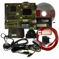
R0K572030S000BE Renesas Electronics America, R0K572030S000BE Datasheet - Page 420

R0K572030S000BE
Manufacturer Part Number
R0K572030S000BE
Description
KIT DEV FOR SH7203
Manufacturer
Renesas Electronics America
Series
Renesas Starter Kits (RSK)r
Type
MCUr
Specifications of R0K572030S000BE
Contents
CPU Board, LCD Module, E10A-Lite Emulator, Cable, QuickStart Guide and CD-ROM
Silicon Manufacturer
Renesas
Kit Contents
Board
Silicon Family Name
SH7203
Silicon Core Number
R5S72030W200FP
Tool / Board Applications
General Purpose MCU, MPU, DSP, DSC
Mcu Supported Families
SH7203
Lead Free Status / RoHS Status
Contains lead / RoHS non-compliant
For Use With/related Products
SH7203
Lead Free Status / Rohs Status
Compliant
- Current page: 420 of 1686
- Download datasheet (10Mb)
Section 9 Bus State Controller (BSC)
the high-impedance state at subsequent rising edges of CKIO. Bus request signals are sampled at
the falling edge of CKIO. Note that CKE, RASU, RASL, CASU, and CASL can be continued to
be driven at the previous value even in the bus-released state by setting the HIZCNT bit in
CMNCR.
The sequence for reclaiming the bus mastership from an external device is described below. 1.5
cycles after the negation of BREQ is detected at the falling edge of CKIO, the bus control signals
are driven high. The bus acknowledge signal is negated at the next falling edge of the clock. The
fastest timing at which actual bus cycles can be resumed after bus control signal assertion is at the
rising edge of the CKIO where address and data signals are driven. Figure 9.55 shows the bus
arbitration timing.
When it is necessary to refresh SDRAM while releasing the bus mastership, the bus mastership
should be returned using the REFOUT signal. For details on the selection of REFOUT, see section
25, Pin Function Controller (PFC). The REFOUT signal is kept asserting at low level until the bus
mastership is acquired. The BREQ signal is negated by asserting the REFOUT signal and the bus
mastership is returned from the external device. If the bus mastership is not returned for a
refreshing period or longer, the contents of SDRAM cannot be guaranteed because a refreshing
cannot be executed.
While releasing the bus mastership, the SLEEP instruction (to enter sleep mode, deep standby
mode, or software standby mode), as well as a manual reset, cannot be executed until the LSI
obtains the bus mastership.
The BREQ input signal is ignored in software standby mode or deep standby mode and the BACK
output signal is placed in the high impedance state. If the bus mastership request is required in this
state, the bus mastership must be released by pulling down the BACK pin to enter software
standby mode or deep standby mode.
The bus mastership release (BREQ signal for high level negation) after the bus mastership request
(BREQ signal for low level assertion) must be performed after the bus usage permission (BACK
signal for low level assertion). If the BREQ signal is negated before the BACK signal is asserted,
only one cycle of the BACK signal is asserted depending on the timing of the BREQ signal to be
negated and this may cause a bus contention between the external device and the LSI.
Rev. 3.00 Sep. 28, 2009 Page 388 of 1650
REJ09B0313-0300
Related parts for R0K572030S000BE
Image
Part Number
Description
Manufacturer
Datasheet
Request
R

Part Number:
Description:
KIT STARTER FOR M16C/29
Manufacturer:
Renesas Electronics America
Datasheet:

Part Number:
Description:
KIT STARTER FOR R8C/2D
Manufacturer:
Renesas Electronics America
Datasheet:

Part Number:
Description:
R0K33062P STARTER KIT
Manufacturer:
Renesas Electronics America
Datasheet:

Part Number:
Description:
KIT STARTER FOR R8C/23 E8A
Manufacturer:
Renesas Electronics America
Datasheet:

Part Number:
Description:
KIT STARTER FOR R8C/25
Manufacturer:
Renesas Electronics America
Datasheet:

Part Number:
Description:
KIT STARTER H8S2456 SHARPE DSPLY
Manufacturer:
Renesas Electronics America
Datasheet:

Part Number:
Description:
KIT STARTER FOR R8C38C
Manufacturer:
Renesas Electronics America
Datasheet:

Part Number:
Description:
KIT STARTER FOR R8C35C
Manufacturer:
Renesas Electronics America
Datasheet:

Part Number:
Description:
KIT STARTER FOR R8CL3AC+LCD APPS
Manufacturer:
Renesas Electronics America
Datasheet:

Part Number:
Description:
KIT STARTER FOR RX610
Manufacturer:
Renesas Electronics America
Datasheet:

Part Number:
Description:
KIT STARTER FOR R32C/118
Manufacturer:
Renesas Electronics America
Datasheet:

Part Number:
Description:
KIT DEV RSK-R8C/26-29
Manufacturer:
Renesas Electronics America
Datasheet:

Part Number:
Description:
KIT STARTER FOR SH7124
Manufacturer:
Renesas Electronics America
Datasheet:

Part Number:
Description:
KIT STARTER FOR H8SX/1622
Manufacturer:
Renesas Electronics America
Datasheet:

Part Number:
Description:
KIT STARTER FOR R8C/18191A1B
Manufacturer:
Renesas Electronics America
Datasheet:


