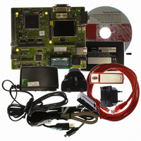
R0K572030S000BE Renesas Electronics America, R0K572030S000BE Datasheet - Page 1466

R0K572030S000BE
Manufacturer Part Number
R0K572030S000BE
Description
KIT DEV FOR SH7203
Manufacturer
Renesas Electronics America
Series
Renesas Starter Kits (RSK)r
Type
MCUr
Specifications of R0K572030S000BE
Contents
CPU Board, LCD Module, E10A-Lite Emulator, Cable, QuickStart Guide and CD-ROM
Silicon Manufacturer
Renesas
Kit Contents
Board
Silicon Family Name
SH7203
Silicon Core Number
R5S72030W200FP
Tool / Board Applications
General Purpose MCU, MPU, DSP, DSC
Mcu Supported Families
SH7203
Lead Free Status / RoHS Status
Contains lead / RoHS non-compliant
For Use With/related Products
SH7203
Lead Free Status / Rohs Status
Compliant
- Current page: 1466 of 1686
- Download datasheet (10Mb)
Section 28 Power-Down Modes
28.3.5
(1)
Setting the standby control register MSTP bits to 1 halts the supply of clocks to the corresponding
on-chip peripheral modules. This function can be used to reduce the power consumption in the
program execution state and sleep mode. Disable a module before placing it in the module standby
mode. In addition, do not access the module's registers while it is in the module standby state.
For details on the states of registers, see section 30.3, Register States in Each Operating Mode.
(2)
The module standby function can be canceled by clearing each MSTP bit to 0, or by a power-on
reset (only possible for RTC, H-UDI, UBC, and DMAC). When taking a module out of the
module standby state by clearing the corresponding MSTP bit to 0, read the MSTP bit to confirm
that it has been cleared to 0.
28.4
28.4.1
When writing to the registers related to power-down modes, note the following.
When writing to the register related to power-down modes, the CPU, after executing a write
instruction, executes the next instruction without waiting for the write operation to complete.
Therefore, to reflect the change specified by writing to the register while the next instruction is
executed, insert a dummy read of the same register between the register write instruction and the
next instruction.
28.4.2
After (1) power-on reset by RES pin is released, and (2) the LSI transits to deep standby mode in
case that bit 7 (CS0KEEPE) and bit 6 (RAMBOOT) of deep standby control register 2 (DSCTR2)
are set to "1", these bits become unable to be written as "0" since then.
To write these as “0”, it is necessary to assert RES pin to low.
Rev. 3.00 Sep. 28, 2009 Page 1434 of 1650
REJ09B0313-0300
Transition to Module Standby Function
Canceling Module Standby Function
Module Standby Function
Usage Notes
Notes on Writing to Registers
Notice about Deep Standby Control Register 2 (DSCTR2)
Related parts for R0K572030S000BE
Image
Part Number
Description
Manufacturer
Datasheet
Request
R

Part Number:
Description:
KIT STARTER FOR M16C/29
Manufacturer:
Renesas Electronics America
Datasheet:

Part Number:
Description:
KIT STARTER FOR R8C/2D
Manufacturer:
Renesas Electronics America
Datasheet:

Part Number:
Description:
R0K33062P STARTER KIT
Manufacturer:
Renesas Electronics America
Datasheet:

Part Number:
Description:
KIT STARTER FOR R8C/23 E8A
Manufacturer:
Renesas Electronics America
Datasheet:

Part Number:
Description:
KIT STARTER FOR R8C/25
Manufacturer:
Renesas Electronics America
Datasheet:

Part Number:
Description:
KIT STARTER H8S2456 SHARPE DSPLY
Manufacturer:
Renesas Electronics America
Datasheet:

Part Number:
Description:
KIT STARTER FOR R8C38C
Manufacturer:
Renesas Electronics America
Datasheet:

Part Number:
Description:
KIT STARTER FOR R8C35C
Manufacturer:
Renesas Electronics America
Datasheet:

Part Number:
Description:
KIT STARTER FOR R8CL3AC+LCD APPS
Manufacturer:
Renesas Electronics America
Datasheet:

Part Number:
Description:
KIT STARTER FOR RX610
Manufacturer:
Renesas Electronics America
Datasheet:

Part Number:
Description:
KIT STARTER FOR R32C/118
Manufacturer:
Renesas Electronics America
Datasheet:

Part Number:
Description:
KIT DEV RSK-R8C/26-29
Manufacturer:
Renesas Electronics America
Datasheet:

Part Number:
Description:
KIT STARTER FOR SH7124
Manufacturer:
Renesas Electronics America
Datasheet:

Part Number:
Description:
KIT STARTER FOR H8SX/1622
Manufacturer:
Renesas Electronics America
Datasheet:

Part Number:
Description:
KIT STARTER FOR R8C/18191A1B
Manufacturer:
Renesas Electronics America
Datasheet:


