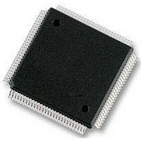
MC912D60CCPVE Freescale Semiconductor, MC912D60CCPVE Datasheet - Page 298

MC912D60CCPVE
Manufacturer Part Number
MC912D60CCPVE
Description
IC MCU 16BIT 112-LQFP
Manufacturer
Freescale Semiconductor
Series
HC12r
Datasheet
1.MC912D60ACFUE8.pdf
(460 pages)
Specifications of MC912D60CCPVE
Core Processor
CPU12
Core Size
16-Bit
Speed
8MHz
Connectivity
CAN, MI Bus, SCI, SPI
Peripherals
POR, PWM, WDT
Number Of I /o
68
Program Memory Size
60KB (60K x 8)
Program Memory Type
FLASH
Eeprom Size
1K x 8
Ram Size
2K x 8
Voltage - Supply (vcc/vdd)
4.5 V ~ 5.5 V
Data Converters
A/D 16x8/10b
Oscillator Type
Internal
Operating Temperature
-40°C ~ 85°C
Package / Case
112-LQFP
Processor Series
HC912D
Core
HC12
Data Bus Width
16 bit
Data Ram Size
2 KB
Interface Type
CAN, SCI, SPI
Maximum Clock Frequency
8 MHz
Number Of Programmable I/os
86
Maximum Operating Temperature
+ 85 C
Mounting Style
SMD/SMT
3rd Party Development Tools
EWHCS12
Minimum Operating Temperature
- 40 C
On-chip Adc
10 bit, 8 Channel
Lead Free Status / RoHS Status
Lead free / RoHS Compliant
Available stocks
Company
Part Number
Manufacturer
Quantity
Price
Company:
Part Number:
MC912D60CCPVE
Manufacturer:
FREESCAL
Quantity:
203
Company:
Part Number:
MC912D60CCPVE
Manufacturer:
Freescale Semiconductor
Quantity:
10 000
- Current page: 298 of 460
- Download datasheet (5Mb)
Freescale Interconnect Bus
SC0CR2 — MI Bus Control Register 2
Technical Data
298
RESET:
Bit 7
—
0
—
6
0
PT — MI Bus TxD0 polarity
Read or write anytime.
RIE — Receiver Interrupt Enable
TE — Transmitter Enable
RE — Receiver Enable
SBK — Send Break
If parity is enabled, this bit determines even or odd parity for both the
receiver and the transmitter.
OR does not generate an interrupt request in MI Bus mode.
When an MI Bus wire is held low for eight or more time slots an
internal circuit on any slave device connected to the bus may reset or
preset the device with default values.
0 = MI Bus transmit pin functions normally.
1 = MI Bus transmit pin will send inverted data.
0 = RDRF interrupt disabled.
1 = MI Bus interrupt will be requested whenever the RDRF status
0 = Transmitter disabled.
1 = MI Bus transmit logic is enabled and the TxD0 pin (Port S bit 1)
0 = Receiver disabled.
1 = Port pin dedicated to the MI Bus; the receiver is enabled by a
0 = No action.
1 = MI transmit line is set low for 20 time slots.
RIE
5
0
flag is set.
is dedicated to the transmitter.
pull sync and is inhibited during a push field.
Freescale Interconnect Bus
—
4
0
TE
3
0
RE
2
0
MC68HC912D60A — Rev. 3.1
—
1
0
Freescale Semiconductor
Bit 0
SBK
0
$00C3
Related parts for MC912D60CCPVE
Image
Part Number
Description
Manufacturer
Datasheet
Request
R
Part Number:
Description:
Manufacturer:
Freescale Semiconductor, Inc
Datasheet:
Part Number:
Description:
Manufacturer:
Freescale Semiconductor, Inc
Datasheet:
Part Number:
Description:
Manufacturer:
Freescale Semiconductor, Inc
Datasheet:
Part Number:
Description:
Manufacturer:
Freescale Semiconductor, Inc
Datasheet:
Part Number:
Description:
Manufacturer:
Freescale Semiconductor, Inc
Datasheet:
Part Number:
Description:
Manufacturer:
Freescale Semiconductor, Inc
Datasheet:
Part Number:
Description:
Manufacturer:
Freescale Semiconductor, Inc
Datasheet:
Part Number:
Description:
Manufacturer:
Freescale Semiconductor, Inc
Datasheet:
Part Number:
Description:
Manufacturer:
Freescale Semiconductor, Inc
Datasheet:
Part Number:
Description:
Manufacturer:
Freescale Semiconductor, Inc
Datasheet:
Part Number:
Description:
Manufacturer:
Freescale Semiconductor, Inc
Datasheet:
Part Number:
Description:
Manufacturer:
Freescale Semiconductor, Inc
Datasheet:
Part Number:
Description:
Manufacturer:
Freescale Semiconductor, Inc
Datasheet:
Part Number:
Description:
Manufacturer:
Freescale Semiconductor, Inc
Datasheet:
Part Number:
Description:
Manufacturer:
Freescale Semiconductor, Inc
Datasheet:


