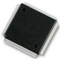
MC912D60CCPVE Freescale Semiconductor, MC912D60CCPVE Datasheet - Page 98

MC912D60CCPVE
Manufacturer Part Number
MC912D60CCPVE
Description
IC MCU 16BIT 112-LQFP
Manufacturer
Freescale Semiconductor
Series
HC12r
Datasheet
1.MC912D60ACFUE8.pdf
(460 pages)
Specifications of MC912D60CCPVE
Core Processor
CPU12
Core Size
16-Bit
Speed
8MHz
Connectivity
CAN, MI Bus, SCI, SPI
Peripherals
POR, PWM, WDT
Number Of I /o
68
Program Memory Size
60KB (60K x 8)
Program Memory Type
FLASH
Eeprom Size
1K x 8
Ram Size
2K x 8
Voltage - Supply (vcc/vdd)
4.5 V ~ 5.5 V
Data Converters
A/D 16x8/10b
Oscillator Type
Internal
Operating Temperature
-40°C ~ 85°C
Package / Case
112-LQFP
Processor Series
HC912D
Core
HC12
Data Bus Width
16 bit
Data Ram Size
2 KB
Interface Type
CAN, SCI, SPI
Maximum Clock Frequency
8 MHz
Number Of Programmable I/os
86
Maximum Operating Temperature
+ 85 C
Mounting Style
SMD/SMT
3rd Party Development Tools
EWHCS12
Minimum Operating Temperature
- 40 C
On-chip Adc
10 bit, 8 Channel
Lead Free Status / RoHS Status
Lead free / RoHS Compliant
Available stocks
Company
Part Number
Manufacturer
Quantity
Price
Company:
Part Number:
MC912D60CCPVE
Manufacturer:
FREESCAL
Quantity:
203
Company:
Part Number:
MC912D60CCPVE
Manufacturer:
Freescale Semiconductor
Quantity:
10 000
- Current page: 98 of 460
- Download datasheet (5Mb)
Flash Memory
7.3 Overview
7.4 Flash EEPROM Control Block
7.5 Flash EEPROM Arrays
Technical Data
98
The Flash EEPROM array is arranged in a 16-bit configuration and may
be read as either bytes, aligned words or misaligned words. Access time
is one bus cycle for byte and aligned word access and two bus cycles for
misaligned word operations.
The Flash EEPROM module supports bulk erase only.
Each Flash EEPROM module has hardware interlocks which protect
stored data from accidental corruption. An erase- and program-
protected 8-Kbyte block for boot routines is located at $6000–$7FFF or
$E000–$FFFF depending upon the mapped location of the Flash
EEPROM arrays.
On 1L02H and later mask sets, an optional protection scheme is
supported to protect the entire two Flash EEPROM modules (32-Kbyte
and 28-Kbyte) against accident program or erase. This is achieved using
the protection bit FPOPEN in EEPROM EEMCR (see
protection bit
A 4-byte register block for each module controls the Flash EEPROM
operation. Configuration information is specified and programmed
independently from the contents of the Flash EEPROM array.
After reset, the control register block for the 32K Flash EEPROM array
(FEE32) is located from addresses $00F4 to $00F7 and for the 28K
Flash EEPROM array (FEE28) from $00F8 to $00FB.
After reset, the 32K Flash EEPROM array is located from addresses
$8000 to $FFFF and the 28K Flash EEPROM array is from $1000 to
$7FFF. In expanded modes, the Flash EEPROM arrays are turned off.
The Flash EEPROM can be mapped to an alternate address range. See
Operating Modes and Resource
FPOPEN).
Flash Memory
Mapping.
MC68HC912D60A — Rev. 3.1
Freescale Semiconductor
7.11 Flash
Related parts for MC912D60CCPVE
Image
Part Number
Description
Manufacturer
Datasheet
Request
R
Part Number:
Description:
Manufacturer:
Freescale Semiconductor, Inc
Datasheet:
Part Number:
Description:
Manufacturer:
Freescale Semiconductor, Inc
Datasheet:
Part Number:
Description:
Manufacturer:
Freescale Semiconductor, Inc
Datasheet:
Part Number:
Description:
Manufacturer:
Freescale Semiconductor, Inc
Datasheet:
Part Number:
Description:
Manufacturer:
Freescale Semiconductor, Inc
Datasheet:
Part Number:
Description:
Manufacturer:
Freescale Semiconductor, Inc
Datasheet:
Part Number:
Description:
Manufacturer:
Freescale Semiconductor, Inc
Datasheet:
Part Number:
Description:
Manufacturer:
Freescale Semiconductor, Inc
Datasheet:
Part Number:
Description:
Manufacturer:
Freescale Semiconductor, Inc
Datasheet:
Part Number:
Description:
Manufacturer:
Freescale Semiconductor, Inc
Datasheet:
Part Number:
Description:
Manufacturer:
Freescale Semiconductor, Inc
Datasheet:
Part Number:
Description:
Manufacturer:
Freescale Semiconductor, Inc
Datasheet:
Part Number:
Description:
Manufacturer:
Freescale Semiconductor, Inc
Datasheet:
Part Number:
Description:
Manufacturer:
Freescale Semiconductor, Inc
Datasheet:
Part Number:
Description:
Manufacturer:
Freescale Semiconductor, Inc
Datasheet:


