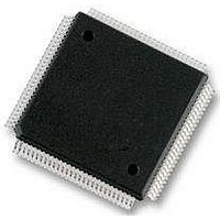
MC912D60CCPVE Freescale Semiconductor, MC912D60CCPVE Datasheet - Page 390

MC912D60CCPVE
Manufacturer Part Number
MC912D60CCPVE
Description
IC MCU 16BIT 112-LQFP
Manufacturer
Freescale Semiconductor
Series
HC12r
Datasheet
1.MC912D60ACFUE8.pdf
(460 pages)
Specifications of MC912D60CCPVE
Core Processor
CPU12
Core Size
16-Bit
Speed
8MHz
Connectivity
CAN, MI Bus, SCI, SPI
Peripherals
POR, PWM, WDT
Number Of I /o
68
Program Memory Size
60KB (60K x 8)
Program Memory Type
FLASH
Eeprom Size
1K x 8
Ram Size
2K x 8
Voltage - Supply (vcc/vdd)
4.5 V ~ 5.5 V
Data Converters
A/D 16x8/10b
Oscillator Type
Internal
Operating Temperature
-40°C ~ 85°C
Package / Case
112-LQFP
Processor Series
HC912D
Core
HC12
Data Bus Width
16 bit
Data Ram Size
2 KB
Interface Type
CAN, SCI, SPI
Maximum Clock Frequency
8 MHz
Number Of Programmable I/os
86
Maximum Operating Temperature
+ 85 C
Mounting Style
SMD/SMT
3rd Party Development Tools
EWHCS12
Minimum Operating Temperature
- 40 C
On-chip Adc
10 bit, 8 Channel
Lead Free Status / RoHS Status
Lead free / RoHS Compliant
Available stocks
Company
Part Number
Manufacturer
Quantity
Price
Company:
Part Number:
MC912D60CCPVE
Manufacturer:
FREESCAL
Quantity:
203
Company:
Part Number:
MC912D60CCPVE
Manufacturer:
Freescale Semiconductor
Quantity:
10 000
- Current page: 390 of 460
- Download datasheet (5Mb)
Development Support
19.4.5.2 INSTRUCTION - Hardware Instruction Decode
INSTRUCTION — BDM Instruction Register (hardware command explanation)
Technical Data
390
RESET:
BIT 7
H/F
0
DATA
6
0
CLKSW — BDMCLK Clock Switch
The WRITE_BD_BYTE@FF01 command that changes CLKSW
including 150 cycles after the data portion of the command should be
timed at the old speed. Beginning with the start of the next BDM
command, the new clock can be used for timing BDM communications.
If ECLK rate is slower than BDMCLK rate, CLKSW is ignored and BDM
system is forced to operate with ECLK.
The INSTRUCTION register is written by the BDM hardware as a result
of serial data shifted in on the BKGD pin. It is readable and writable in
Special Peripheral mode on the parallel bus. It is discussed here for two
conditions: when a hardware command is executed and when a
firmware command is executed.
Read and write: all modes
The hardware clears the INSTRUCTION register if 512 BDMCLK cycles
occur between falling edges from the host.
The bits in the BDM instruction register have the following meanings
when a hardware command is executed.
H/F — Hardware/Firmware Flag
0 = BDM system operates with BCLK.
1 = BDM system operates with ECLK.
0 = Firmware command
1 = Hardware command
R/W
5
0
Development Support
BKGND
4
0
W/B
3
0
BD/U
2
0
MC68HC912D60A — Rev. 3.1
1
0
0
Freescale Semiconductor
BIT 0
0
0
$FF00
Related parts for MC912D60CCPVE
Image
Part Number
Description
Manufacturer
Datasheet
Request
R
Part Number:
Description:
Manufacturer:
Freescale Semiconductor, Inc
Datasheet:
Part Number:
Description:
Manufacturer:
Freescale Semiconductor, Inc
Datasheet:
Part Number:
Description:
Manufacturer:
Freescale Semiconductor, Inc
Datasheet:
Part Number:
Description:
Manufacturer:
Freescale Semiconductor, Inc
Datasheet:
Part Number:
Description:
Manufacturer:
Freescale Semiconductor, Inc
Datasheet:
Part Number:
Description:
Manufacturer:
Freescale Semiconductor, Inc
Datasheet:
Part Number:
Description:
Manufacturer:
Freescale Semiconductor, Inc
Datasheet:
Part Number:
Description:
Manufacturer:
Freescale Semiconductor, Inc
Datasheet:
Part Number:
Description:
Manufacturer:
Freescale Semiconductor, Inc
Datasheet:
Part Number:
Description:
Manufacturer:
Freescale Semiconductor, Inc
Datasheet:
Part Number:
Description:
Manufacturer:
Freescale Semiconductor, Inc
Datasheet:
Part Number:
Description:
Manufacturer:
Freescale Semiconductor, Inc
Datasheet:
Part Number:
Description:
Manufacturer:
Freescale Semiconductor, Inc
Datasheet:
Part Number:
Description:
Manufacturer:
Freescale Semiconductor, Inc
Datasheet:
Part Number:
Description:
Manufacturer:
Freescale Semiconductor, Inc
Datasheet:


