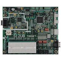
LFEBS12UB Freescale Semiconductor, LFEBS12UB Datasheet - Page 1151

LFEBS12UB
Manufacturer Part Number
LFEBS12UB
Description
KIT STUDENT LEARNING S12 DG128
Manufacturer
Freescale Semiconductor
Specifications of LFEBS12UB
Architecture
8/16-bit
Code Gen Tools Included
Code Warrior
Silicon Manufacturer
Freescale
Core Architecture
S12
Core Sub-architecture
S12
Silicon Core Number
MC9S12
Silicon Family Name
S12D
Kit Contents
HCS12 DG128 Learning Kit
Rohs Compliant
Yes
Lead Free Status / RoHS Status
Lead free / RoHS Compliant
- Current page: 1151 of 1328
- Download datasheet (9Mb)
The Full Partition D-Flash command (see
information register fields where address 0x12_0000 defines the D-Flash partition for user access and
address 0x12_0004 defines the buffer RAM partition for EEE operations.
Freescale Semiconductor
Buffer RAM START = 0x13_F000
Buffer RAM END = 0x13_FFFF
D-Flash START = 0x10_0000
D-Flash END = 0x10_7FFF
MC9S12XE-Family Reference Manual , Rev. 1.23
Figure 29-3. EEE Resource Memory Map
0x13_FEC0
0x13_FFC0
0x12_FFFF
0x13_FE00
0x13_FE40
0x13_FE80
0x12_E000
0x13_FF00
0x13_FF40
0x13_FF80
0x12_0000
0x12_1000
0x12_2000
0x12_4000
Section
29.4.2.15) is used to program the EEE nonvolatile
Chapter 29 1024 KByte Flash Module (S12XFTM1024K5V2)
EEE Nonvolatile Information Register (EEEIFRON)
128 bytes
EEE Tag RAM (TMGRAMON)
256 bytes
Memory Controller Scratch RAM (TMGRAMON)
1024 bytes
D-Flash User Partition
D-Flash EEE Partition
D-Flash Memory
32 Kbytes
Buffer RAM User Partition
Buffer RAM EEE Partition
Protectable Region (EEE only)
64, 128, 192, 256, 320, 384, 448, 512 bytes
Buffer RAM
4 Kbytes
1151
Related parts for LFEBS12UB
Image
Part Number
Description
Manufacturer
Datasheet
Request
R
Part Number:
Description:
Manufacturer:
Freescale Semiconductor, Inc
Datasheet:
Part Number:
Description:
Manufacturer:
Freescale Semiconductor, Inc
Datasheet:
Part Number:
Description:
Manufacturer:
Freescale Semiconductor, Inc
Datasheet:
Part Number:
Description:
Manufacturer:
Freescale Semiconductor, Inc
Datasheet:
Part Number:
Description:
Manufacturer:
Freescale Semiconductor, Inc
Datasheet:
Part Number:
Description:
Manufacturer:
Freescale Semiconductor, Inc
Datasheet:
Part Number:
Description:
Manufacturer:
Freescale Semiconductor, Inc
Datasheet:
Part Number:
Description:
Manufacturer:
Freescale Semiconductor, Inc
Datasheet:
Part Number:
Description:
Manufacturer:
Freescale Semiconductor, Inc
Datasheet:
Part Number:
Description:
Manufacturer:
Freescale Semiconductor, Inc
Datasheet:
Part Number:
Description:
Manufacturer:
Freescale Semiconductor, Inc
Datasheet:
Part Number:
Description:
Manufacturer:
Freescale Semiconductor, Inc
Datasheet:
Part Number:
Description:
Manufacturer:
Freescale Semiconductor, Inc
Datasheet:
Part Number:
Description:
Manufacturer:
Freescale Semiconductor, Inc
Datasheet:
Part Number:
Description:
Manufacturer:
Freescale Semiconductor, Inc
Datasheet:


