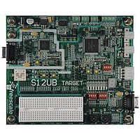
LFEBS12UB Freescale Semiconductor, LFEBS12UB Datasheet - Page 75

LFEBS12UB
Manufacturer Part Number
LFEBS12UB
Description
KIT STUDENT LEARNING S12 DG128
Manufacturer
Freescale Semiconductor
Specifications of LFEBS12UB
Architecture
8/16-bit
Code Gen Tools Included
Code Warrior
Silicon Manufacturer
Freescale
Core Architecture
S12
Core Sub-architecture
S12
Silicon Core Number
MC9S12
Silicon Family Name
S12D
Kit Contents
HCS12 DG128 Learning Kit
Rohs Compliant
Yes
Lead Free Status / RoHS Status
Lead free / RoHS Compliant
- Current page: 75 of 1328
- Download datasheet (9Mb)
1.3
The clock and reset generator module (CRG) provides the internal clock signals for the core and all
peripheral modules.
Consult the CRG specification for details on clock generation.
The system clock can be supplied in several ways enabling a range of system operating frequencies to be
supported:
The clock generated by the PLL or oscillator provides the main system clock frequencies core clock and
bus clock. As shown in
the memories, and the peripherals.
Freescale Semiconductor
Because of an order from the United States International Trade Commission, BGA-packaged product lines and partnumbers
indicated here currently are not available from Freescale for import or sale in the United States prior to September 2010
•
•
•
EXTAL
XTAL
The on-chip phase locked loop (PLL)
the PLL self clocking
the oscillator
System Clock Description
SCI0 . . SCI 7
Bus Clock
RAM
CRG
Figure 1-9
Figure
SPI0 . . SPI2
1-9, these system clocks are used throughout the MCU to drive the core,
shows the clock connections from the CRG to all modules.
MC9S12XE-Family Reference Manual Rev. 1.23
S12X
Figure 1-9. Clock Connections
Core Clock
CAN0 . . CAN4
XGATE
Oscillator Clock
IIC0 & IIC1
FLASH &
Chapter 1 Device Overview MC9S12XE-Family
EEE
ATD0 & ATD1
PIT
ECT
PIM
PWM
TIM
75
Related parts for LFEBS12UB
Image
Part Number
Description
Manufacturer
Datasheet
Request
R
Part Number:
Description:
Manufacturer:
Freescale Semiconductor, Inc
Datasheet:
Part Number:
Description:
Manufacturer:
Freescale Semiconductor, Inc
Datasheet:
Part Number:
Description:
Manufacturer:
Freescale Semiconductor, Inc
Datasheet:
Part Number:
Description:
Manufacturer:
Freescale Semiconductor, Inc
Datasheet:
Part Number:
Description:
Manufacturer:
Freescale Semiconductor, Inc
Datasheet:
Part Number:
Description:
Manufacturer:
Freescale Semiconductor, Inc
Datasheet:
Part Number:
Description:
Manufacturer:
Freescale Semiconductor, Inc
Datasheet:
Part Number:
Description:
Manufacturer:
Freescale Semiconductor, Inc
Datasheet:
Part Number:
Description:
Manufacturer:
Freescale Semiconductor, Inc
Datasheet:
Part Number:
Description:
Manufacturer:
Freescale Semiconductor, Inc
Datasheet:
Part Number:
Description:
Manufacturer:
Freescale Semiconductor, Inc
Datasheet:
Part Number:
Description:
Manufacturer:
Freescale Semiconductor, Inc
Datasheet:
Part Number:
Description:
Manufacturer:
Freescale Semiconductor, Inc
Datasheet:
Part Number:
Description:
Manufacturer:
Freescale Semiconductor, Inc
Datasheet:
Part Number:
Description:
Manufacturer:
Freescale Semiconductor, Inc
Datasheet:


