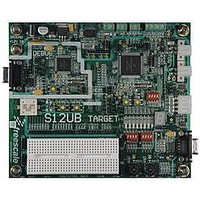
LFEBS12UB Freescale Semiconductor, LFEBS12UB Datasheet - Page 1226

LFEBS12UB
Manufacturer Part Number
LFEBS12UB
Description
KIT STUDENT LEARNING S12 DG128
Manufacturer
Freescale Semiconductor
Specifications of LFEBS12UB
Architecture
8/16-bit
Code Gen Tools Included
Code Warrior
Silicon Manufacturer
Freescale
Core Architecture
S12
Core Sub-architecture
S12
Silicon Core Number
MC9S12
Silicon Family Name
S12D
Kit Contents
HCS12 DG128 Learning Kit
Rohs Compliant
Yes
Lead Free Status / RoHS Status
Lead free / RoHS Compliant
- Current page: 1226 of 1328
- Download datasheet (9Mb)
Appendix A Electrical Characteristics
A.3
A.3.1
The time base for all NVM program or erase operations is derived from the oscillator. A minimum
oscillator frequency f
do not have any means to monitor the frequency and will not prevent program or erase operation at
frequencies above or below the specified minimum. When attempting to program or erase the NVM
modules at a lower frequency, a full program or erase transition is not assured.
The program and erase operations are timed using a clock derived from the oscillator using the FCLKDIV
register. The frequency of this clock must be set within the limits specified as f
The minimum program and erase times shown in
maximum f
A.3.1.1
The time it takes to perform a blank check is dependant on the location of the first non-blank word starting
at relative address zero. It takes one bus cycle per phrase to verify plus a setup of the command. Assuming
that no non blank location is found, then the erase verify all blocks is given by.
A.3.1.2
The time it takes to perform a blank check is dependant on the location of the first non-blank word starting
at relative address zero. It takes one bus cycle per phrase to verify plus a setup of the command. Assuming
that no non blank location is found, then the erase verify time for a single 256K NVM array is given by
For a 128K NVM or D-Flash array the erase verify time is given by
A.3.1.3
The maximum time depends on the number of phrases being verified (N
1226
3
t
t
t
t
check
check
check
check
These values include the quantization error which is inherently 1/2 count for any A/D converter.
=
=
=
=
NVM, Flash and Emulated EEPROM
NVMBUS
Timing Parameters
33500
33500
17200
(
752
Erase Verify All Blocks (Blank Check) (FCMD=0x01)
Erase Verify Block (Blank Check) (FCMD=0x02)
Erase Verify P-Flash Section (FCMD=0x03)
+
⋅
⋅
⋅
N
unless otherwise shown. The maximum times are calculated for minimum f
--------------------- -
f
--------------------- -
f
--------------------- -
f
NVMOSC
NVMBUS
NVMBUS
NVMBUS
VP
)
1
1
1
⋅
--------------------- -
f
NVMBUS
is required for performing program or erase operations. The NVM modules
MC9S12XE-Family Reference Manual , Rev. 1.23
1
Table A-19
are calculated for maximum f
VP
)
NVMOP
Freescale Semiconductor
.
NVMOP
NVMOP
and
Related parts for LFEBS12UB
Image
Part Number
Description
Manufacturer
Datasheet
Request
R
Part Number:
Description:
Manufacturer:
Freescale Semiconductor, Inc
Datasheet:
Part Number:
Description:
Manufacturer:
Freescale Semiconductor, Inc
Datasheet:
Part Number:
Description:
Manufacturer:
Freescale Semiconductor, Inc
Datasheet:
Part Number:
Description:
Manufacturer:
Freescale Semiconductor, Inc
Datasheet:
Part Number:
Description:
Manufacturer:
Freescale Semiconductor, Inc
Datasheet:
Part Number:
Description:
Manufacturer:
Freescale Semiconductor, Inc
Datasheet:
Part Number:
Description:
Manufacturer:
Freescale Semiconductor, Inc
Datasheet:
Part Number:
Description:
Manufacturer:
Freescale Semiconductor, Inc
Datasheet:
Part Number:
Description:
Manufacturer:
Freescale Semiconductor, Inc
Datasheet:
Part Number:
Description:
Manufacturer:
Freescale Semiconductor, Inc
Datasheet:
Part Number:
Description:
Manufacturer:
Freescale Semiconductor, Inc
Datasheet:
Part Number:
Description:
Manufacturer:
Freescale Semiconductor, Inc
Datasheet:
Part Number:
Description:
Manufacturer:
Freescale Semiconductor, Inc
Datasheet:
Part Number:
Description:
Manufacturer:
Freescale Semiconductor, Inc
Datasheet:
Part Number:
Description:
Manufacturer:
Freescale Semiconductor, Inc
Datasheet:


