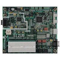
LFEBS12UB Freescale Semiconductor, LFEBS12UB Datasheet - Page 1236

LFEBS12UB
Manufacturer Part Number
LFEBS12UB
Description
KIT STUDENT LEARNING S12 DG128
Manufacturer
Freescale Semiconductor
Specifications of LFEBS12UB
Architecture
8/16-bit
Code Gen Tools Included
Code Warrior
Silicon Manufacturer
Freescale
Core Architecture
S12
Core Sub-architecture
S12
Silicon Core Number
MC9S12
Silicon Family Name
S12D
Kit Contents
HCS12 DG128 Learning Kit
Rohs Compliant
Yes
Lead Free Status / RoHS Status
Lead free / RoHS Compliant
- Current page: 1236 of 1328
- Download datasheet (9Mb)
Appendix A Electrical Characteristics
A.5.1
The voltage regulator is intended to supply the internal logic and oscillator. It allows no external DC loads.
A.5.2
The capacitive loads are specified in
A.5.3
LVI (low voltage interrupt), POR (power-on reset) and LVRs (low voltage reset) handle chip power-up or
drops of the supply voltage. Their function is shown in
1236
Num
1
3
V
LVRX
PORD
LVI
V
POR
VDD/VDDF external capacitive load
VDDPLL external capacitive load
Resistive Loads
Capacitive Loads
Chip Power-up and Voltage Drops
Figure A-3. MC9S12XE-Family - Chip Power-up and Voltage Drops (not scaled)
V
V
V
V
LVID
LVIA
LVRXD
LVRXA
Characteristic
MC9S12XE-Family Reference Manual , Rev. 1.23
Table A-22. - Required Capacitive Loads
Table
A-22. Ceramic capacitors with X7R dielectricum are required.
C
Symbol
C
DDPLLext
DDext
V
DDX
Figure A-3
Min
176
LVI enabled LVI disabled due to LVR
80
.
Recommended
220
220
Freescale Semiconductor
Max
264
264
V
DD
t
Unit
nF
nF
Related parts for LFEBS12UB
Image
Part Number
Description
Manufacturer
Datasheet
Request
R
Part Number:
Description:
Manufacturer:
Freescale Semiconductor, Inc
Datasheet:
Part Number:
Description:
Manufacturer:
Freescale Semiconductor, Inc
Datasheet:
Part Number:
Description:
Manufacturer:
Freescale Semiconductor, Inc
Datasheet:
Part Number:
Description:
Manufacturer:
Freescale Semiconductor, Inc
Datasheet:
Part Number:
Description:
Manufacturer:
Freescale Semiconductor, Inc
Datasheet:
Part Number:
Description:
Manufacturer:
Freescale Semiconductor, Inc
Datasheet:
Part Number:
Description:
Manufacturer:
Freescale Semiconductor, Inc
Datasheet:
Part Number:
Description:
Manufacturer:
Freescale Semiconductor, Inc
Datasheet:
Part Number:
Description:
Manufacturer:
Freescale Semiconductor, Inc
Datasheet:
Part Number:
Description:
Manufacturer:
Freescale Semiconductor, Inc
Datasheet:
Part Number:
Description:
Manufacturer:
Freescale Semiconductor, Inc
Datasheet:
Part Number:
Description:
Manufacturer:
Freescale Semiconductor, Inc
Datasheet:
Part Number:
Description:
Manufacturer:
Freescale Semiconductor, Inc
Datasheet:
Part Number:
Description:
Manufacturer:
Freescale Semiconductor, Inc
Datasheet:
Part Number:
Description:
Manufacturer:
Freescale Semiconductor, Inc
Datasheet:


