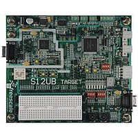
LFEBS12UB Freescale Semiconductor, LFEBS12UB Datasheet - Page 576

LFEBS12UB
Manufacturer Part Number
LFEBS12UB
Description
KIT STUDENT LEARNING S12 DG128
Manufacturer
Freescale Semiconductor
Specifications of LFEBS12UB
Architecture
8/16-bit
Code Gen Tools Included
Code Warrior
Silicon Manufacturer
Freescale
Core Architecture
S12
Core Sub-architecture
S12
Silicon Core Number
MC9S12
Silicon Family Name
S12D
Kit Contents
HCS12 DG128 Learning Kit
Rohs Compliant
Yes
Lead Free Status / RoHS Status
Lead free / RoHS Compliant
- Current page: 576 of 1328
- Download datasheet (9Mb)
Chapter 14 Enhanced Capture Timer (ECT16B8CV3)
14.4.1.1.3
There are four delay counters in this module associated with IC channels 0–3. The use of this feature is
explained in the diagram and notes below.
In
576
Because of an order from the United States International Trade Commission, BGA-packaged product lines and partnumbers
Figure 14-74
indicated here currently are not available from Freescale for import or sale in the United States prior to September 2010
2. IC Queue Mode (LATQ = 0)
1. Input pulses with a duration of (DLY_CNT – 1) cycles or shorter are rejected.
2. Input pulses with a duration between (DLY_CNT – 1) and DLY_CNT cycles may be rejected or
If the corresponding NOVWx bit of the ICOVW register is set, the capture register or its holding
register cannot be written by an event unless they are empty (see
This will prevent the captured value from being overwritten until it is read or latched in the holding
register.
The main timer value is memorized in the IC register by a valid input pin transition (see
69
If the corresponding NOVWx bit of the ICOVW register is cleared, with a new occurrence of a
capture, the value of the IC register will be transferred to its holding register and the IC register
memorizes the new timer value.
If the corresponding NOVWx bit of the ICOVW register is set, the capture register or its holding
register cannot be written by an event unless they are empty (see
if the TFMOD bit of the ICSYS register is set,the timer flags C3F--C0F in TFLG register are set
only when a latch on the corresponding holding register occurs,after C3F--C0F are set,user should
clear flag C3F--C0F,then read TCx and TCxH to make TCx and TCxH be empty.
In queue mode, reads of the holding register will latch the corresponding pulse accumulator value
to its holding register.
accepted, depending on their relative alignment with the sample points.
and
BUS CLOCK
Figure
Delayed IC Channels
INPUT ON
INPUT ON
INPUT ON
INPUT ON
DLY_CNT
a delay counter value of 256 bus cycles is considered.
CH0–3
CH0–3
CH0–3
CH0–3
Figure 14-74. Channel Input Validity with Delay Counter Feature
14-70).
0
MC9S12XE-Family Reference Manual Rev. 1.23
1
2
255.5 Cycles
255.5 Cycles
255 Cycles
256 Cycles
3
253
254
255
Section 14.4.1.1, “IC
Section 14.4.1.1, “IC
256
Accepted
Rejected
Rejected
Accepted
Freescale Semiconductor
Channels”).
Channels”).
Figure 14-
Related parts for LFEBS12UB
Image
Part Number
Description
Manufacturer
Datasheet
Request
R
Part Number:
Description:
Manufacturer:
Freescale Semiconductor, Inc
Datasheet:
Part Number:
Description:
Manufacturer:
Freescale Semiconductor, Inc
Datasheet:
Part Number:
Description:
Manufacturer:
Freescale Semiconductor, Inc
Datasheet:
Part Number:
Description:
Manufacturer:
Freescale Semiconductor, Inc
Datasheet:
Part Number:
Description:
Manufacturer:
Freescale Semiconductor, Inc
Datasheet:
Part Number:
Description:
Manufacturer:
Freescale Semiconductor, Inc
Datasheet:
Part Number:
Description:
Manufacturer:
Freescale Semiconductor, Inc
Datasheet:
Part Number:
Description:
Manufacturer:
Freescale Semiconductor, Inc
Datasheet:
Part Number:
Description:
Manufacturer:
Freescale Semiconductor, Inc
Datasheet:
Part Number:
Description:
Manufacturer:
Freescale Semiconductor, Inc
Datasheet:
Part Number:
Description:
Manufacturer:
Freescale Semiconductor, Inc
Datasheet:
Part Number:
Description:
Manufacturer:
Freescale Semiconductor, Inc
Datasheet:
Part Number:
Description:
Manufacturer:
Freescale Semiconductor, Inc
Datasheet:
Part Number:
Description:
Manufacturer:
Freescale Semiconductor, Inc
Datasheet:
Part Number:
Description:
Manufacturer:
Freescale Semiconductor, Inc
Datasheet:


