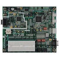
LFEBS12UB Freescale Semiconductor, LFEBS12UB Datasheet - Page 272

LFEBS12UB
Manufacturer Part Number
LFEBS12UB
Description
KIT STUDENT LEARNING S12 DG128
Manufacturer
Freescale Semiconductor
Specifications of LFEBS12UB
Architecture
8/16-bit
Code Gen Tools Included
Code Warrior
Silicon Manufacturer
Freescale
Core Architecture
S12
Core Sub-architecture
S12
Silicon Core Number
MC9S12
Silicon Family Name
S12D
Kit Contents
HCS12 DG128 Learning Kit
Rohs Compliant
Yes
Lead Free Status / RoHS Status
Lead free / RoHS Compliant
- Current page: 272 of 1328
- Download datasheet (9Mb)
Chapter 6 Interrupt (S12XINTV2)
6.3.2.3
Read: Anytime
Write: Anytime
6.3.2.4
The eight register window visible at addresses INT_CFDATA0–7 contains the configuration data for the
block of eight interrupt requests (out of 128) selected by the interrupt configuration address register
(INT_CFADDR) in ascending order. INT_CFDATA0 represents the interrupt configuration data register
of the vector with the lowest address in this block, while INT_CFDATA7 represents the interrupt
configuration data register of the vector with the highest address, respectively.
272
Address: 0x0127
INT_CFADDR[7:4]
Because of an order from the United States International Trade Commission, BGA-packaged product lines and partnumbers
Reset
indicated here currently are not available from Freescale for import or sale in the United States prior to September 2010
W
Field
R
7–4
Interrupt Request Configuration Address Register (INT_CFADDR)
Interrupt Request Configuration Data Registers (INT_CFDATA0–7)
0
7
Priority
Interrupt Request Configuration Data Register Select Bits — These bits determine which of the 128
configuration data registers are accessible in the 8 register window at INT_CFDATA0–7. The hexadecimal
value written to this register corresponds to the upper nibble of the lower byte of the address of the interrupt
vector, i.e., writing 0xE0 to this register selects the configuration data register block for the 8 interrupt vector
requests starting with vector at address (vector base + 0x00E0) to be accessible as INT_CFDATA0–7.
Note: Writing all 0s selects non-existing configuration registers. In this case write accesses to
high
low
Figure 6-5. Interrupt Configuration Address Register (INT_CFADDR)
= Unimplemented or Reserved
INT_CFDATA0–7 will be ignored and read accesses will return all 0.
INT_CFADDR[7:4]
0
6
XILVL2
0
0
0
0
1
1
1
1
MC9S12XE-Family Reference Manual , Rev. 1.23
Table 6-7. INT_CFADDR Field Descriptions
Table 6-6. XGATE Interrupt Priority Levels
XILVL1
5
0
0
0
1
1
0
0
1
1
XILVL0
1
4
0
1
0
1
0
1
0
1
Description
Interrupt request is disabled
0
0
3
Priority level 1
Priority level 2
Priority level 3
Priority level 4
Priority level 5
Priority level 6
Priority level 7
Meaning
2
0
0
Freescale Semiconductor
0
0
1
0
0
0
Related parts for LFEBS12UB
Image
Part Number
Description
Manufacturer
Datasheet
Request
R
Part Number:
Description:
Manufacturer:
Freescale Semiconductor, Inc
Datasheet:
Part Number:
Description:
Manufacturer:
Freescale Semiconductor, Inc
Datasheet:
Part Number:
Description:
Manufacturer:
Freescale Semiconductor, Inc
Datasheet:
Part Number:
Description:
Manufacturer:
Freescale Semiconductor, Inc
Datasheet:
Part Number:
Description:
Manufacturer:
Freescale Semiconductor, Inc
Datasheet:
Part Number:
Description:
Manufacturer:
Freescale Semiconductor, Inc
Datasheet:
Part Number:
Description:
Manufacturer:
Freescale Semiconductor, Inc
Datasheet:
Part Number:
Description:
Manufacturer:
Freescale Semiconductor, Inc
Datasheet:
Part Number:
Description:
Manufacturer:
Freescale Semiconductor, Inc
Datasheet:
Part Number:
Description:
Manufacturer:
Freescale Semiconductor, Inc
Datasheet:
Part Number:
Description:
Manufacturer:
Freescale Semiconductor, Inc
Datasheet:
Part Number:
Description:
Manufacturer:
Freescale Semiconductor, Inc
Datasheet:
Part Number:
Description:
Manufacturer:
Freescale Semiconductor, Inc
Datasheet:
Part Number:
Description:
Manufacturer:
Freescale Semiconductor, Inc
Datasheet:
Part Number:
Description:
Manufacturer:
Freescale Semiconductor, Inc
Datasheet:


