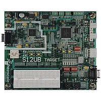
LFEBS12UB Freescale Semiconductor, LFEBS12UB Datasheet - Page 905

LFEBS12UB
Manufacturer Part Number
LFEBS12UB
Description
KIT STUDENT LEARNING S12 DG128
Manufacturer
Freescale Semiconductor
Specifications of LFEBS12UB
Architecture
8/16-bit
Code Gen Tools Included
Code Warrior
Silicon Manufacturer
Freescale
Core Architecture
S12
Core Sub-architecture
S12
Silicon Core Number
MC9S12
Silicon Family Name
S12D
Kit Contents
HCS12 DG128 Learning Kit
Rohs Compliant
Yes
Lead Free Status / RoHS Status
Lead free / RoHS Compliant
- Current page: 905 of 1328
- Download datasheet (9Mb)
25.3.2.1
The FCLKDIV register is used to control timed events in program and erase algorithms.
All bits in the FCLKDIV register are readable, bits 6–0 are write once and bit 7 is not writable.
Freescale Semiconductor
FDIV[6:0]
FDIVLD
Address
Offset Module Base + 0x0000
Reset
& Name
Field
6–0
7
W
R
FDIVLD
Clock Divider Loaded
0 FCLKDIV register has not been written
1 FCLKDIV register has been written since the last reset
Clock Divider Bits — FDIV[6:0] must be set to effectively divide OSCCLK down to generate an internal Flash
clock, FCLK, with a target frequency of 1 MHz for use by the Flash module to control timed events during program
and erase algorithms.
Please refer to
Flash Clock Divider Register (FCLKDIV)
0
7
The FCLKDIV register should never be written while a Flash command is
executing (CCIF=0). The FCLKDIV register is writable during the Flash
reset sequence even though CCIF is clear.
= Unimplemented or Reserved
7
Section 25.4.1, “Flash Command Operations,”
Figure 25-4. FTM256K2 Register Summary (continued)
0
6
Figure 25-5. Flash Clock Divider Register (FCLKDIV)
= Unimplemented or Reserved
Table 25-9
MC9S12XE-Family Reference Manual , Rev. 1.23
6
Table 25-8. FCLKDIV Field Descriptions
0
5
shows recommended values for FDIV[6:0] based on OSCCLK frequency.
5
CAUTION
0
4
Description
4
FDIV[6:0]
Chapter 25 256 KByte Flash Module (S12XFTM256K2V1)
0
3
for more information.
3
0
2
2
0
1
1
0
0
0
905
Related parts for LFEBS12UB
Image
Part Number
Description
Manufacturer
Datasheet
Request
R
Part Number:
Description:
Manufacturer:
Freescale Semiconductor, Inc
Datasheet:
Part Number:
Description:
Manufacturer:
Freescale Semiconductor, Inc
Datasheet:
Part Number:
Description:
Manufacturer:
Freescale Semiconductor, Inc
Datasheet:
Part Number:
Description:
Manufacturer:
Freescale Semiconductor, Inc
Datasheet:
Part Number:
Description:
Manufacturer:
Freescale Semiconductor, Inc
Datasheet:
Part Number:
Description:
Manufacturer:
Freescale Semiconductor, Inc
Datasheet:
Part Number:
Description:
Manufacturer:
Freescale Semiconductor, Inc
Datasheet:
Part Number:
Description:
Manufacturer:
Freescale Semiconductor, Inc
Datasheet:
Part Number:
Description:
Manufacturer:
Freescale Semiconductor, Inc
Datasheet:
Part Number:
Description:
Manufacturer:
Freescale Semiconductor, Inc
Datasheet:
Part Number:
Description:
Manufacturer:
Freescale Semiconductor, Inc
Datasheet:
Part Number:
Description:
Manufacturer:
Freescale Semiconductor, Inc
Datasheet:
Part Number:
Description:
Manufacturer:
Freescale Semiconductor, Inc
Datasheet:
Part Number:
Description:
Manufacturer:
Freescale Semiconductor, Inc
Datasheet:
Part Number:
Description:
Manufacturer:
Freescale Semiconductor, Inc
Datasheet:


