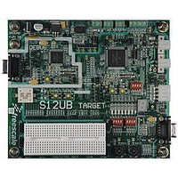
LFEBS12UB Freescale Semiconductor, LFEBS12UB Datasheet - Page 639

LFEBS12UB
Manufacturer Part Number
LFEBS12UB
Description
KIT STUDENT LEARNING S12 DG128
Manufacturer
Freescale Semiconductor
Specifications of LFEBS12UB
Architecture
8/16-bit
Code Gen Tools Included
Code Warrior
Silicon Manufacturer
Freescale
Core Architecture
S12
Core Sub-architecture
S12
Silicon Core Number
MC9S12
Silicon Family Name
S12D
Kit Contents
HCS12 DG128 Learning Kit
Rohs Compliant
Yes
Lead Free Status / RoHS Status
Lead free / RoHS Compliant
- Current page: 639 of 1328
- Download datasheet (9Mb)
16.3.3.2
The eight data segment registers, each with bits DB[7:0], contain the data to be transmitted or received.
The number of bytes to be transmitted or received is determined by the data length code in the
corresponding DLR register.
Module Base + 0x00X4 to Module Base + 0x00XB
Freescale Semiconductor
Module Base + 0x00X2
Module Base + 0x00X3
DB[7:0]
Field
7-0
Reset:
Reset:
Reset:
W
W
R
R
Figure 16-34. Data Segment Registers (DSR0–DSR7) — Extended Identifier Mapping
W
R
Data bits 7-0
Data Segment Registers (DSR0-7)
7
x
7
x
DB7
7
x
Figure 16-32. Identifier Register 2 — Standard Mapping
Figure 16-33. Identifier Register 3 — Standard Mapping
= Unused; always read ‘x’
= Unused; always read ‘x’
Table 16-33. DSR0–DSR7 Register Field Descriptions
6
x
6
x
DB6
x
6
MC9S12XE-Family Reference Manual Rev. 1.23
5
x
5
x
DB5
5
x
Chapter 16 Freescale’s Scalable Controller Area Network (S12MSCANV3)
4
x
4
x
DB4
Description
4
x
x
x
DB3
3
3
x
3
DB2
2
x
2
x
2
x
DB1
x
x
1
1
1
x
DB0
0
x
0
x
x
0
639
Related parts for LFEBS12UB
Image
Part Number
Description
Manufacturer
Datasheet
Request
R
Part Number:
Description:
Manufacturer:
Freescale Semiconductor, Inc
Datasheet:
Part Number:
Description:
Manufacturer:
Freescale Semiconductor, Inc
Datasheet:
Part Number:
Description:
Manufacturer:
Freescale Semiconductor, Inc
Datasheet:
Part Number:
Description:
Manufacturer:
Freescale Semiconductor, Inc
Datasheet:
Part Number:
Description:
Manufacturer:
Freescale Semiconductor, Inc
Datasheet:
Part Number:
Description:
Manufacturer:
Freescale Semiconductor, Inc
Datasheet:
Part Number:
Description:
Manufacturer:
Freescale Semiconductor, Inc
Datasheet:
Part Number:
Description:
Manufacturer:
Freescale Semiconductor, Inc
Datasheet:
Part Number:
Description:
Manufacturer:
Freescale Semiconductor, Inc
Datasheet:
Part Number:
Description:
Manufacturer:
Freescale Semiconductor, Inc
Datasheet:
Part Number:
Description:
Manufacturer:
Freescale Semiconductor, Inc
Datasheet:
Part Number:
Description:
Manufacturer:
Freescale Semiconductor, Inc
Datasheet:
Part Number:
Description:
Manufacturer:
Freescale Semiconductor, Inc
Datasheet:
Part Number:
Description:
Manufacturer:
Freescale Semiconductor, Inc
Datasheet:
Part Number:
Description:
Manufacturer:
Freescale Semiconductor, Inc
Datasheet:


