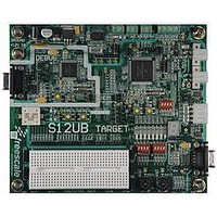
LFEBS12UB Freescale Semiconductor, LFEBS12UB Datasheet - Page 793

LFEBS12UB
Manufacturer Part Number
LFEBS12UB
Description
KIT STUDENT LEARNING S12 DG128
Manufacturer
Freescale Semiconductor
Specifications of LFEBS12UB
Architecture
8/16-bit
Code Gen Tools Included
Code Warrior
Silicon Manufacturer
Freescale
Core Architecture
S12
Core Sub-architecture
S12
Silicon Core Number
MC9S12
Silicon Family Name
S12D
Kit Contents
HCS12 DG128 Learning Kit
Rohs Compliant
Yes
Lead Free Status / RoHS Status
Lead free / RoHS Compliant
- Current page: 793 of 1328
- Download datasheet (9Mb)
22.2
The TIM16B8CV2 module has a total of eight external pins.
22.2.1
This pin serves as input capture or output compare for channel 7. This can also be configured as pulse
accumulator input.
22.2.2
This pin serves as input capture or output compare for channel 6.
22.2.3
This pin serves as input capture or output compare for channel 5.
22.2.4
This pin serves as input capture or output compare for channel 4. Pin
22.2.5
This pin serves as input capture or output compare for channel 3.
22.2.6
This pin serves as input capture or output compare for channel 2.
Freescale Semiconductor
Because of an order from the United States International Trade Commission, BGA-packaged product lines and partnumbers
indicated here currently are not available from Freescale for import or sale in the United States prior to September 2010
External Signal Description
IOC7 — Input Capture and Output Compare Channel 7 Pin
IOC6 — Input Capture and Output Compare Channel 6 Pin
IOC5 — Input Capture and Output Compare Channel 5 Pin
IOC4 — Input Capture and Output Compare Channel 4 Pin
IOC3 — Input Capture and Output Compare Channel 3 Pin
IOC2 — Input Capture and Output Compare Channel 2 Pin
CHANNEL 7 OUTPUT COMPARE
Figure 22-4. Channel 7 Output Compare/Pulse Accumulator Logic
TIOS7
TEN
PULSE
ACCUMULATOR
OCPD
MC9S12XE-Family Reference Manual Rev. 1.23
Chapter 22 Timer Module (TIM16B8CV2) Block Description
PAD
793
Related parts for LFEBS12UB
Image
Part Number
Description
Manufacturer
Datasheet
Request
R
Part Number:
Description:
Manufacturer:
Freescale Semiconductor, Inc
Datasheet:
Part Number:
Description:
Manufacturer:
Freescale Semiconductor, Inc
Datasheet:
Part Number:
Description:
Manufacturer:
Freescale Semiconductor, Inc
Datasheet:
Part Number:
Description:
Manufacturer:
Freescale Semiconductor, Inc
Datasheet:
Part Number:
Description:
Manufacturer:
Freescale Semiconductor, Inc
Datasheet:
Part Number:
Description:
Manufacturer:
Freescale Semiconductor, Inc
Datasheet:
Part Number:
Description:
Manufacturer:
Freescale Semiconductor, Inc
Datasheet:
Part Number:
Description:
Manufacturer:
Freescale Semiconductor, Inc
Datasheet:
Part Number:
Description:
Manufacturer:
Freescale Semiconductor, Inc
Datasheet:
Part Number:
Description:
Manufacturer:
Freescale Semiconductor, Inc
Datasheet:
Part Number:
Description:
Manufacturer:
Freescale Semiconductor, Inc
Datasheet:
Part Number:
Description:
Manufacturer:
Freescale Semiconductor, Inc
Datasheet:
Part Number:
Description:
Manufacturer:
Freescale Semiconductor, Inc
Datasheet:
Part Number:
Description:
Manufacturer:
Freescale Semiconductor, Inc
Datasheet:
Part Number:
Description:
Manufacturer:
Freescale Semiconductor, Inc
Datasheet:


