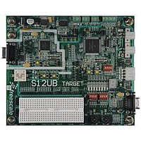
LFEBS12UB Freescale Semiconductor, LFEBS12UB Datasheet - Page 69

LFEBS12UB
Manufacturer Part Number
LFEBS12UB
Description
KIT STUDENT LEARNING S12 DG128
Manufacturer
Freescale Semiconductor
Specifications of LFEBS12UB
Architecture
8/16-bit
Code Gen Tools Included
Code Warrior
Silicon Manufacturer
Freescale
Core Architecture
S12
Core Sub-architecture
S12
Silicon Core Number
MC9S12
Silicon Family Name
S12D
Kit Contents
HCS12 DG128 Learning Kit
Rohs Compliant
Yes
Lead Free Status / RoHS Status
Lead free / RoHS Compliant
- Current page: 69 of 1328
- Download datasheet (9Mb)
1.2.3.52
PM7 is a general-purpose input or output pin. It can be configured as the transmit pin TXCAN of the
scalable controller area network controller 3 or 4 (CAN3 or CAN4). PM7 can be configured as the transmit
pin TXD3 of the serial communication interface 3 (SCI3).
1.2.3.53
PM6 is a general-purpose input or output pin. It can be configured as the receive pin RXCAN of the
scalable controller area network controller 3 or 4 (CAN3 or CAN4). PM6 can be configured as the receive
pin RXD3 of the serial communication interface 3 (SCI3).
1.2.3.54
PM5 is a general-purpose input or output pin. It can be configured as the transmit pin TXCAN of the
scalable controller area network controllers 0, 2 or 4 (CAN0, CAN2, or CAN4). It can be configured as
the serial clock pin SCK of the serial peripheral interface 0 (SPI0).
1.2.3.55
PM4 is a general-purpose input or output pin. It can be configured as the receive pin RXCAN of the
scalable controller area network controllers 0, 2, or 4 (CAN0, CAN2, or CAN4). It can be configured as
the master output (during master mode) or slave input pin (during slave mode) MOSI for the serial
peripheral interface 0 (SPI0).
1.2.3.56
PM3 is a general-purpose input or output pin. It can be configured as the transmit pin TXCAN of the
scalable controller area network controllers 1 or 0 (CAN1 or CAN0). It can be configured as the slave
select pin SS of the serial peripheral interface 0 (SPI0).
1.2.3.57
PM2 is a general-purpose input or output pin. It can be configured as the receive pin RXCAN of the
scalable controller area network controllers 1 or 0 (CAN1 or CAN0). It can be configured as the master
input (during master mode) or slave output pin (during slave mode) MISO for the serial peripheral
interface 0 (SPI0).
1.2.3.58
PM1 is a general-purpose input or output pin. It can be configured as the transmit pin TXCAN of the
scalable controller area network controller 0 (CAN0).
1.2.3.59
PM0 is a general-purpose input or output pin. It can be configured as the receive pin RXCAN of the
scalable controller area network controller 0 (CAN0).
Freescale Semiconductor
Because of an order from the United States International Trade Commission, BGA-packaged product lines and partnumbers
indicated here currently are not available from Freescale for import or sale in the United States prior to September 2010
PM7 / TXCAN3 / TXCAN4 / TXD3 — Port M I/O Pin 7
PM6 / RXCAN3 / RXCAN4 / RXD3 — Port M I/O Pin 6
PM5 / TXCAN0 / TXCAN2 / TXCAN4 / SCK0 — Port M I/O Pin 5
PM4 / RXCAN0 / RXCAN2 / RXCAN4 / MOSI0 — Port M I/O Pin 4
PM3 / TXCAN1 / TXCAN0 / SS0 — Port M I/O Pin 3
PM2 / RXCAN1 / RXCAN0 / MISO0 — Port M I/O Pin 2
PM1 / TXCAN0 — Port M I/O Pin 1
PM0 / RXCAN0 — Port M I/O Pin 0
MC9S12XE-Family Reference Manual Rev. 1.23
Chapter 1 Device Overview MC9S12XE-Family
69
Related parts for LFEBS12UB
Image
Part Number
Description
Manufacturer
Datasheet
Request
R
Part Number:
Description:
Manufacturer:
Freescale Semiconductor, Inc
Datasheet:
Part Number:
Description:
Manufacturer:
Freescale Semiconductor, Inc
Datasheet:
Part Number:
Description:
Manufacturer:
Freescale Semiconductor, Inc
Datasheet:
Part Number:
Description:
Manufacturer:
Freescale Semiconductor, Inc
Datasheet:
Part Number:
Description:
Manufacturer:
Freescale Semiconductor, Inc
Datasheet:
Part Number:
Description:
Manufacturer:
Freescale Semiconductor, Inc
Datasheet:
Part Number:
Description:
Manufacturer:
Freescale Semiconductor, Inc
Datasheet:
Part Number:
Description:
Manufacturer:
Freescale Semiconductor, Inc
Datasheet:
Part Number:
Description:
Manufacturer:
Freescale Semiconductor, Inc
Datasheet:
Part Number:
Description:
Manufacturer:
Freescale Semiconductor, Inc
Datasheet:
Part Number:
Description:
Manufacturer:
Freescale Semiconductor, Inc
Datasheet:
Part Number:
Description:
Manufacturer:
Freescale Semiconductor, Inc
Datasheet:
Part Number:
Description:
Manufacturer:
Freescale Semiconductor, Inc
Datasheet:
Part Number:
Description:
Manufacturer:
Freescale Semiconductor, Inc
Datasheet:
Part Number:
Description:
Manufacturer:
Freescale Semiconductor, Inc
Datasheet:


