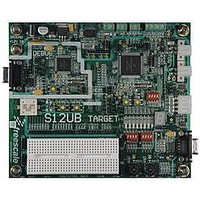
LFEBS12UB Freescale Semiconductor, LFEBS12UB Datasheet - Page 325

LFEBS12UB
Manufacturer Part Number
LFEBS12UB
Description
KIT STUDENT LEARNING S12 DG128
Manufacturer
Freescale Semiconductor
Specifications of LFEBS12UB
Architecture
8/16-bit
Code Gen Tools Included
Code Warrior
Silicon Manufacturer
Freescale
Core Architecture
S12
Core Sub-architecture
S12
Silicon Core Number
MC9S12
Silicon Family Name
S12D
Kit Contents
HCS12 DG128 Learning Kit
Rohs Compliant
Yes
Lead Free Status / RoHS Status
Lead free / RoHS Compliant
- Current page: 325 of 1328
- Download datasheet (9Mb)
Table 8-31
tagged operations since the trigger occurs based on the tagged opcode reaching the execution stage of the
instruction queue. Thus these bits are ignored if tagged triggering is selected.
8.3.2.8.2
Read: Anytime. See
Write: If DBG not armed. See
Freescale Semiconductor
Address: 0x0029
Because of an order from the United States International Trade Commission, BGA-packaged product lines and partnumbers
Bit[22:16]
Reset
indicated here currently are not available from Freescale for import or sale in the United States prior to September 2010
Field
COMPE
6–0
Field
SRC
W
R
1
0
shows the effect for RWE and RW on the comparison conditions. These bits are not useful for
Comparator Address High Compare Bits — The Comparator address high compare bits control whether the
selected comparator will compare the address bus bits [22:16] to a logic one or logic zero. This register byte is
ignored for XGATE compares.
0 Compare corresponding address bit to a logic zero
1 Compare corresponding address bit to a logic one
0
0
7
Debug Comparator Address High Register (DBGXAH)
Determines mapping of comparator to CPU12X or XGATE
0 The comparator is mapped to CPU12X buses
1 The comparator is mapped to XGATE address and data buses
Determines if comparator is enabled
0 The comparator is not enabled
1 The comparator is enabled for state sequence triggers or tag generation
RWE Bit
Figure 8-15. Debug Comparator Address High Register (DBGXAH)
Table 8-29
0
0
1
1
1
1
= Unimplemented or Reserved
Bit 22
0
6
Table 8-30. DBGXCTL Field Descriptions (continued)
Table 8-31. Read or Write Comparison Logic Table
RW Bit
Table 8-29
MC9S12XE-Family Reference Manual Rev. 1.23
for visible register encoding.
0
0
1
1
x
x
Table 8-32. DBGXAH Field Descriptions
Bit 21
5
0
RW Signal
for visible register encoding.
0
1
0
1
0
1
Bit 20
0
4
Description
Description
Bit 19
RW not used in comparison
RW not used in comparison
0
3
Comment
No match
No match
Chapter 8 S12X Debug (S12XDBGV3) Module
Write
Read
Bit 18
2
0
Bit 17
0
1
Bit 16
0
0
325
Related parts for LFEBS12UB
Image
Part Number
Description
Manufacturer
Datasheet
Request
R
Part Number:
Description:
Manufacturer:
Freescale Semiconductor, Inc
Datasheet:
Part Number:
Description:
Manufacturer:
Freescale Semiconductor, Inc
Datasheet:
Part Number:
Description:
Manufacturer:
Freescale Semiconductor, Inc
Datasheet:
Part Number:
Description:
Manufacturer:
Freescale Semiconductor, Inc
Datasheet:
Part Number:
Description:
Manufacturer:
Freescale Semiconductor, Inc
Datasheet:
Part Number:
Description:
Manufacturer:
Freescale Semiconductor, Inc
Datasheet:
Part Number:
Description:
Manufacturer:
Freescale Semiconductor, Inc
Datasheet:
Part Number:
Description:
Manufacturer:
Freescale Semiconductor, Inc
Datasheet:
Part Number:
Description:
Manufacturer:
Freescale Semiconductor, Inc
Datasheet:
Part Number:
Description:
Manufacturer:
Freescale Semiconductor, Inc
Datasheet:
Part Number:
Description:
Manufacturer:
Freescale Semiconductor, Inc
Datasheet:
Part Number:
Description:
Manufacturer:
Freescale Semiconductor, Inc
Datasheet:
Part Number:
Description:
Manufacturer:
Freescale Semiconductor, Inc
Datasheet:
Part Number:
Description:
Manufacturer:
Freescale Semiconductor, Inc
Datasheet:
Part Number:
Description:
Manufacturer:
Freescale Semiconductor, Inc
Datasheet:


