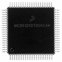
MC9S12XDT256CAA Freescale Semiconductor, MC9S12XDT256CAA Datasheet - Page 581

MC9S12XDT256CAA
Manufacturer Part Number
MC9S12XDT256CAA
Description
IC MCU 256K FLASH 80-QFP
Manufacturer
Freescale Semiconductor
Series
HCS12r
Datasheet
1.MC9S12XD64CAA.pdf
(1348 pages)
Specifications of MC9S12XDT256CAA
Core Processor
HCS12X
Core Size
16-Bit
Speed
80MHz
Connectivity
CAN, EBI/EMI, I²C, IrDA, LIN, SCI, SPI
Peripherals
LVD, POR, PWM, WDT
Number Of I /o
59
Program Memory Size
256KB (256K x 8)
Program Memory Type
FLASH
Eeprom Size
4K x 8
Ram Size
16K x 8
Voltage - Supply (vcc/vdd)
2.35 V ~ 5.5 V
Data Converters
A/D 8x10b
Oscillator Type
External
Operating Temperature
-40°C ~ 85°C
Package / Case
80-QFP
Processor Series
S12XD
Core
HCS12
Data Bus Width
16 bit
Data Ram Size
16 KB
Interface Type
CAN/I2C/SCI/SPI
Maximum Clock Frequency
40 MHz
Number Of Programmable I/os
59
Number Of Timers
12
Maximum Operating Temperature
+ 85 C
Mounting Style
SMD/SMT
3rd Party Development Tools
EWHCS12
Development Tools By Supplier
EVB9S12XDP512E
Minimum Operating Temperature
- 40 C
On-chip Adc
8-ch x 10-bit
Lead Free Status / RoHS Status
Lead free / RoHS Compliant
Available stocks
Company
Part Number
Manufacturer
Quantity
Price
Company:
Part Number:
MC9S12XDT256CAA
Manufacturer:
Freescale Semiconductor
Quantity:
10 000
Company:
Part Number:
MC9S12XDT256CAAR
Manufacturer:
Freescale Semiconductor
Quantity:
10 000
- Current page: 581 of 1348
- Download datasheet (8Mb)
1
2
3
Freescale Semiconductor
READ_NEXT
READ_PC
READ_D
READ_X
READ_Y
READ_SP
WRITE_NEXT<f-hel
vetica><st-superscri
pt>
WRITE_PC
WRITE_D
WRITE_X
WRITE_Y
WRITE_SP
GO
GO_UNTIL
TRACE1
TAGGO -> GO
If enabled, ACK will occur when data is ready for transmission for all BDM READ commands and will occur after the write is
complete for all BDM WRITE commands.
are accessed rather than user code. Writing BDM firmware is not possible.
System stop disables the ACK function and ignored commands will not have an ACK-pulse (e.g., CPU in stop or wait mode).
The GO_UNTIL command will not get an Acknowledge if CPU executes the wait or stop instruction before the “UNTIL”
condition (BDM active again) is reached (see
When the firmware command READ_NEXT or WRITE_NEXT is used to access the BDM address space the BDM resources
Command
3
2
1
Opcode
(hex)
0C
62
63
64
65
66
67
42
43
44
45
46
47
08
10
18
16-bit data out Increment X index register by 2 (X = X + 2), then read word X points to.
16-bit data out Read program counter.
16-bit data out Read D accumulator.
16-bit data out Read X index register.
16-bit data out Read Y index register.
16-bit data out Read stack pointer.
16-bit data in
16-bit data in
16-bit data in
16-bit data in
16-bit data in
16-bit data in
Data
none
none
none
none
MC9S12XDP512 Data Sheet, Rev. 2.21
Table 15-6. Firmware Commands
Section 15.4.7, “Serial Interface Hardware Handshake Protocol”
Increment X index register by 2 (X = X + 2), then write word to location
pointed to by X.
Write program counter.
Write D accumulator.
Write X index register.
Write Y index register.
Write stack pointer.
Go to user program. If enabled, ACK will occur when leaving active
background mode.
Go to user program. If enabled, ACK will occur upon returning to active
background mode.
Execute one user instruction then return to active BDM. If enabled,
ACK will occur upon returning to active background mode.
(Previous enable tagging and go to user program.)
This command will be deprecated and should not be used anymore.
Opcode will be executed as a GO command.
Chapter 15 Background Debug Module (S12XBDMV2)
Description
last Note).
581
Related parts for MC9S12XDT256CAA
Image
Part Number
Description
Manufacturer
Datasheet
Request
R

Part Number:
Description:
16-BIT MICROPROCESSOR FAMILY
Manufacturer:
FREESCALE [Freescale Semiconductor, Inc]
Datasheet:
Part Number:
Description:
Manufacturer:
Freescale Semiconductor, Inc
Datasheet:
Part Number:
Description:
Manufacturer:
Freescale Semiconductor, Inc
Datasheet:
Part Number:
Description:
Manufacturer:
Freescale Semiconductor, Inc
Datasheet:
Part Number:
Description:
Manufacturer:
Freescale Semiconductor, Inc
Datasheet:
Part Number:
Description:
Manufacturer:
Freescale Semiconductor, Inc
Datasheet:
Part Number:
Description:
Manufacturer:
Freescale Semiconductor, Inc
Datasheet:
Part Number:
Description:
Manufacturer:
Freescale Semiconductor, Inc
Datasheet:
Part Number:
Description:
Manufacturer:
Freescale Semiconductor, Inc
Datasheet:
Part Number:
Description:
Manufacturer:
Freescale Semiconductor, Inc
Datasheet:
Part Number:
Description:
Manufacturer:
Freescale Semiconductor, Inc
Datasheet:
Part Number:
Description:
Manufacturer:
Freescale Semiconductor, Inc
Datasheet:
Part Number:
Description:
Manufacturer:
Freescale Semiconductor, Inc
Datasheet:
Part Number:
Description:
Manufacturer:
Freescale Semiconductor, Inc
Datasheet:
Part Number:
Description:
Manufacturer:
Freescale Semiconductor, Inc
Datasheet:


