DS3163 Maxim Integrated Products, DS3163 Datasheet - Page 113

DS3163
Manufacturer Part Number
DS3163
Description
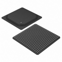
IC TRPL ATM/PACKET PHY 400-PBGA
Manufacturer
Maxim Integrated Products
Datasheet
1.DS3163.pdf
(384 pages)
Specifications of DS3163
Applications
*
Mounting Type
Surface Mount
Package / Case
400-BGA
Lead Free Status / RoHS Status
Lead free / RoHS Compliant
Available stocks
Company
Part Number
Manufacturer
Quantity
Price
- Current page: 113 of 384
- Download datasheet (4Mb)
Figure 10-9
paths available.
Figure 10-9. Loopback Modes
10.5.1.1 Terminal Loopback (TLB)
Terminal loopback is enabled by setting PORT.CR4.LBM[2:0] = 001. Terminal loopback mode will not be enabled
when the port is configured for loop timed mode (set via the PORT.CR3.LOOPT bit).
The terminal loopback is a loopback as close to the pins as possible.
TDATn,TNEGn / TOHMOn to RLCLKn ,RPOSn / RDATn , RNEGn / ROHMIn.
10.5.1.2 Line Loopback (LLB)
Line loopback is enabled by setting PORT.CR4.LBM[2:0] = X10. DLB and LLB are enabled at the same time when
LBM[2:0] = 110, and only LLB is enabled when LBM[2:0] = 010.
The clock from the RLCLK pin will be output to the TCLKOn pin. The POS and NEG data from the RPOSn and
RNEGn pin will be sampled with the receive clock to time it to the pin interface.
When LLB is enabled, unframed all ones AIS can optionally be automatically enabled on the receive data path.
This AIS signal will be output on the RSERn pin in flexible fractional mode, and sent to the receive cell or packet
processor in framer modes, effectively stopping cell or packet data flow. When DLB and LLB is enabled, the AIS
signal will not be transmitted.
Refer to
10.5.1.3 Payload Loopback (PLB)
Payload loopback is enabled by setting PORT.CR4.LBM[2:0] = 011.
The payload loopback copies the payload data from the receive framer to the transmit framer (before the fractional
logic) which then re-frames the payload before transmission. Payload loopback is operational in all framing modes
except “- OHM” modes.
When PLB is enabled, unframed all ones AIS transmission can optionally be automatically enabled on the receive
data path. This AIS signal will be output on the RSER pin in flexible fractional mode, and sent to the receive cell or
packet processor in framer modes, effectively stopping cell or packet data flow.
In all modes, the TSOFIn input pin is ignored. The external transmit output pins TDENn and TSOFOn/TDENn can
optionally be disabled by forcing a zero when PLB is enabled.
In the framed modes, the data flow from the transmit cell or packet processor can be optionally disabled when PLB
is enabled. If the data flow is not disabled, the cells or packets from the system interface will be discarded. See
Figure
Clock Rate
Adapter
10-9.
Figure
highlights where each loopback mode is located and gives an overall view of the various loopback
10-9.
Encoder
Decoder
B3ZS/
HDB3
HDB3
B3ZS/
TUA1
TAIS
IEEE P1149.1
JTAG Test
Access Port
FEAC
DS3 / E3
DS3 / E3
Receive
Framer
Transmit
Formatter
Buffer
Trace
Trail
HDLC
GEN
UA1
TX FRAC/
PLCP
RX FRAC/
PLCP
Rx Packet
Processor
Processor
RX BERT
Processor
Processor
TX BERT
Tx Packet
Rx Cell
Tx Cell
Microprocessor
Interface
It will loop back TLCLKn,TPOSn /
FIFO
FIFO
Tx
Rx
Related parts for DS3163
Image
Part Number
Description
Manufacturer
Datasheet
Request
R

Part Number:
Description:
MAX7528KCWPMaxim Integrated Products [CMOS Dual 8-Bit Buffered Multiplying DACs]
Manufacturer:
Maxim Integrated Products
Datasheet:

Part Number:
Description:
Single +5V, fully integrated, 1.25Gbps laser diode driver.
Manufacturer:
Maxim Integrated Products
Datasheet:

Part Number:
Description:
Single +5V, fully integrated, 155Mbps laser diode driver.
Manufacturer:
Maxim Integrated Products
Datasheet:

Part Number:
Description:
VRD11/VRD10, K8 Rev F 2/3/4-Phase PWM Controllers with Integrated Dual MOSFET Drivers
Manufacturer:
Maxim Integrated Products
Datasheet:

Part Number:
Description:
Highly Integrated Level 2 SMBus Battery Chargers
Manufacturer:
Maxim Integrated Products
Datasheet:

Part Number:
Description:
Current Monitor and Accumulator with Integrated Sense Resistor; ; Temperature Range: -40°C to +85°C
Manufacturer:
Maxim Integrated Products

Part Number:
Description:
TSSOP 14/A�/RS-485 Transceivers with Integrated 100O/120O Termination Resis
Manufacturer:
Maxim Integrated Products

Part Number:
Description:
TSSOP 14/A�/RS-485 Transceivers with Integrated 100O/120O Termination Resis
Manufacturer:
Maxim Integrated Products

Part Number:
Description:
QFN 16/A�/AC-DC and DC-DC Peak-Current-Mode Converters with Integrated Step
Manufacturer:
Maxim Integrated Products

Part Number:
Description:
TDFN/A/65V, 1A, 600KHZ, SYNCHRONOUS STEP-DOWN REGULATOR WITH INTEGRATED SWI
Manufacturer:
Maxim Integrated Products

Part Number:
Description:
Integrated Temperature Controller f
Manufacturer:
Maxim Integrated Products

Part Number:
Description:
SOT23-6/I�/45MHz to 650MHz, Integrated IF VCOs with Differential Output
Manufacturer:
Maxim Integrated Products

Part Number:
Description:
SOT23-6/I�/45MHz to 650MHz, Integrated IF VCOs with Differential Output
Manufacturer:
Maxim Integrated Products

Part Number:
Description:
EVALUATION KIT/2.4GHZ TO 2.5GHZ 802.11G/B RF TRANSCEIVER WITH INTEGRATED PA
Manufacturer:
Maxim Integrated Products

Part Number:
Description:
QFN/E/DUAL PCIE/SATA HIGH SPEED SWITCH WITH INTEGRATED BIAS RESISTOR
Manufacturer:
Maxim Integrated Products
Datasheet:


