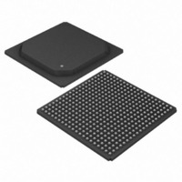
DS3163 Maxim Integrated Products, DS3163 Datasheet - Page 91

DS3163
Manufacturer Part Number
DS3163
Description
IC TRPL ATM/PACKET PHY 400-PBGA
Manufacturer
Maxim Integrated Products
Datasheet
1.DS3163.pdf
(384 pages)
Specifications of DS3163
Applications
*
Mounting Type
Surface Mount
Package / Case
400-BGA
Lead Free Status / RoHS Status
Lead free / RoHS Compliant
Available stocks
Company
Part Number
Manufacturer
Quantity
Price
- Current page: 91 of 384
- Download datasheet (4Mb)
9 INITIALIZATION AND CONFIGURATION
STEP 1: Check Device ID Code:
Before any testing can be done, device ID code, which is stored in GL.IDR, shoud be checked against device ID
codes shown below to ensure correct device is being used.
Current device ID codes are:
STEP 2: Initialize the Device.
Before configuring for operation, make sure the device is in a known condition with all registers set to their default
value by initiating a Global Reset. (See Section 10.3) A Global Reset can be initiated via the RST pin or by the
Global Reset bit (GL.CR1.RST). A Port Reset is not necessary since the global reset includes a reset of all ports to
their default values.
STEP 3: Clear the Reset.
It is necessary to clear the RST bit to begin normal operation.
After clearing the RST bit, the device is configured for default mode.
Default mode:
STEP 4: Clear the Data Path Resets and the Port Power-Down bit.
The default value of the Data Path Resets is one, which keeps the internal logic in the reset status. The user
needs to clear the following bits:
STEP 5: Select the clock source.
STEP 6: Configure the Framing Mode and the Line Mode.
STEP 7: Disable Payload AIS (downstream AIS) and Line AIS
STEP 8: Initialize and configure the FIFOs.
o
o
o
o
System Interface: UTOPIA Level 2, 8-bit databus
Framer: C-bit DS3
GL.CR1.RSTDP = 0
PORT.CR1.RSTDP = 0
PORT.CR1.PD = 0
Loop Time (use the receive clock (RLCLKn)): Set PORT.CR3.LOOPT = 1
CLAD Source: Set PORT.CR3.CLADC = 0
TCLKI Source: Set PORT.CR3.CLADC = 1
If using the CLAD, properly configure the CLAD by setting the CLAD bits in
PORT.CR2.LM = 0 (AMI/B3ZS/HDB3 Interface) or another setting. See
PORT.CR2.FM[5:0] set to the correct framing mode. See
PORT.CR1.PAIS[2:0] = 111
PORT.CR1.LAIS[1:0] = 11
Reset the Transmit and Receive FIFO. FF.TCR.TFRST = 1. FF.RCR.RFRST = 1.
Clear the FIFO Reset bits. FF.TCR.TFRST = 0. FF.RCR.RFRST = 0.
Set the FIFO Transmit Level Control Register and the FIFO Transmit Port Address Control Register.
Set the FIFO Receive Level Control Register and the FIFO Receive Port Address Control Register.
The Port Address needs to be configured to match the master controller address for each port.
DS3161 rev 1.0:
DS3162 rev 1.0:
DS3163 rev 1.0:
DS3164 rev 1.0:
0x40h
0x41h
0x42h
0x43h
Table 10-30.
Table 10-31
GL.CR2.
Related parts for DS3163
Image
Part Number
Description
Manufacturer
Datasheet
Request
R

Part Number:
Description:
MAX7528KCWPMaxim Integrated Products [CMOS Dual 8-Bit Buffered Multiplying DACs]
Manufacturer:
Maxim Integrated Products
Datasheet:

Part Number:
Description:
Single +5V, fully integrated, 1.25Gbps laser diode driver.
Manufacturer:
Maxim Integrated Products
Datasheet:

Part Number:
Description:
Single +5V, fully integrated, 155Mbps laser diode driver.
Manufacturer:
Maxim Integrated Products
Datasheet:

Part Number:
Description:
VRD11/VRD10, K8 Rev F 2/3/4-Phase PWM Controllers with Integrated Dual MOSFET Drivers
Manufacturer:
Maxim Integrated Products
Datasheet:

Part Number:
Description:
Highly Integrated Level 2 SMBus Battery Chargers
Manufacturer:
Maxim Integrated Products
Datasheet:

Part Number:
Description:
Current Monitor and Accumulator with Integrated Sense Resistor; ; Temperature Range: -40°C to +85°C
Manufacturer:
Maxim Integrated Products

Part Number:
Description:
TSSOP 14/A�/RS-485 Transceivers with Integrated 100O/120O Termination Resis
Manufacturer:
Maxim Integrated Products

Part Number:
Description:
TSSOP 14/A�/RS-485 Transceivers with Integrated 100O/120O Termination Resis
Manufacturer:
Maxim Integrated Products

Part Number:
Description:
QFN 16/A�/AC-DC and DC-DC Peak-Current-Mode Converters with Integrated Step
Manufacturer:
Maxim Integrated Products

Part Number:
Description:
TDFN/A/65V, 1A, 600KHZ, SYNCHRONOUS STEP-DOWN REGULATOR WITH INTEGRATED SWI
Manufacturer:
Maxim Integrated Products

Part Number:
Description:
Integrated Temperature Controller f
Manufacturer:
Maxim Integrated Products

Part Number:
Description:
SOT23-6/I�/45MHz to 650MHz, Integrated IF VCOs with Differential Output
Manufacturer:
Maxim Integrated Products

Part Number:
Description:
SOT23-6/I�/45MHz to 650MHz, Integrated IF VCOs with Differential Output
Manufacturer:
Maxim Integrated Products

Part Number:
Description:
EVALUATION KIT/2.4GHZ TO 2.5GHZ 802.11G/B RF TRANSCEIVER WITH INTEGRATED PA
Manufacturer:
Maxim Integrated Products

Part Number:
Description:
QFN/E/DUAL PCIE/SATA HIGH SPEED SWITCH WITH INTEGRATED BIAS RESISTOR
Manufacturer:
Maxim Integrated Products
Datasheet:


