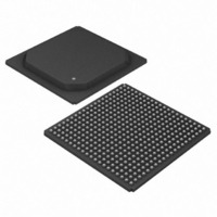
DS3163 Maxim Integrated Products, DS3163 Datasheet - Page 19

DS3163
Manufacturer Part Number
DS3163
Description
IC TRPL ATM/PACKET PHY 400-PBGA
Manufacturer
Maxim Integrated Products
Datasheet
1.DS3163.pdf
(384 pages)
Specifications of DS3163
Applications
*
Mounting Type
Surface Mount
Package / Case
400-BGA
Lead Free Status / RoHS Status
Lead free / RoHS Compliant
Available stocks
Company
Part Number
Manufacturer
Quantity
Price
- Current page: 19 of 384
- Download datasheet (4Mb)
•
•
•
•
•
3.11 Transmit Packet Processor Features
•
•
•
•
•
•
•
•
•
3.12 Transmit PLCP Formatter Features
•
•
•
•
•
•
•
3.13 Transmit DS3/E3 Formatter Features
•
•
•
•
•
•
•
•
•
•
•
•
3.14 Clock Rate Adapter Features
•
•
•
•
Single-bit and multiple-bit header error insertion for diagnostics
Controls include enables/disables/settings for: cell processing, HEC insertion, coset polynomial addition, cell
scrambling, fill cell type, error insertion type/rate/count, HEC bit corruption
Counter for number of cells read from the transmit FIFO
Cell mapping into the DS3/E3 frame, the PLCP frame, an externally defined frame, or the entire line bandwidth
Octet alignment option for externally defined frame formats
FCS calculation (16-bit or 32-bit) and insertion/overwrite
Programmable FCS error insertion for diagnostics
Bit or octet stuffing
Programmable inter-frame fill insertion (flags or all-ones)
Automatic packet abort insertion
Packet scrambling using the self-synchronizing scrambler (x
Controls include enables/disables/settings for: packet processing, FCS insertion or overwrite, 16/32-bit FCS,
inter-frame fill type/length, scrambling, FCS error insertion type/rate/count
Counters for number of packets and bytes read from the transmit FIFO
Octet alignment with octet stuffing option for externally defined frame formats
Insertion of FAS bytes (A1, A2), path overhead identification (POI) bytes, and path overhead bytes
Generation of BIP-8 (B1), FEBE and RAI (G1)
C1 cycle/stuff counter generation referenced to GPIO4 input pin, referenced to the received PLCP timing, or
based on an 8 kHz division of one of the clock sources
Automatic or manual insertion of FAS errors, BIP-8 errors
All path overhead fields can be sourced from the PLCP transmit overhead port
HDLC port for data link messages on F1, M1 or M2 bytes
Trail Trace port for trace messages on F1 byte
Insertion of framing overhead for M23 or C-bit parity DS3,or G.751 E3 or G.832 E3
B3ZS/HDB3 encoding
Generation of RDI, AIS, and DS3 idle signal
Automatic or manual insertion of bipolar violations (BPVs), excessive zeroes (EXZ) occurrences, F-bit errors,
M-bit errors, FAS errors, P-bit parity errors, CP-bit parity errors, BIP-8 errors, and far end block errors (FEBE)
HDLC port for DS3 path maintenance data link (PMDL), G.751 national bit or G.832 NR or GC channels
FEAC port for DS3 FEAC channel can be configured to send one codeword, one codeword continuously, or
two different codewords back-to-back to send DS3 Line Loopback commands
16-byte Trail Trace Buffer port for the G.832 trail access point identifier
Insertion of G.832 payload type, and timing marker bits from registers
DS3 M23 C bits configurable as payload or overhead; as overhead they can be controlled from registers or the
transmit overhead port
Most framing overhead fields can be sourced from transmit overhead port
Formatter bypass mode for clear channel or externally defined format applications
Support for subrate DS3/E3, internally or externally controlled (Fractional DS3/E3)
Generation of the internally needed DS3 (44.736 MHz), E3 (34.368 MHz), and STS-1(51.84 MHz) clocks a
from single input reference clock
Input reference clock can be 51.84 MHz, 44.736MHz or 34.368 MHz
Derived clocks can be transmitted off-chip for external system use
Standards compliant jitter and wander requirements.
43
+1)
Related parts for DS3163
Image
Part Number
Description
Manufacturer
Datasheet
Request
R

Part Number:
Description:
MAX7528KCWPMaxim Integrated Products [CMOS Dual 8-Bit Buffered Multiplying DACs]
Manufacturer:
Maxim Integrated Products
Datasheet:

Part Number:
Description:
Single +5V, fully integrated, 1.25Gbps laser diode driver.
Manufacturer:
Maxim Integrated Products
Datasheet:

Part Number:
Description:
Single +5V, fully integrated, 155Mbps laser diode driver.
Manufacturer:
Maxim Integrated Products
Datasheet:

Part Number:
Description:
VRD11/VRD10, K8 Rev F 2/3/4-Phase PWM Controllers with Integrated Dual MOSFET Drivers
Manufacturer:
Maxim Integrated Products
Datasheet:

Part Number:
Description:
Highly Integrated Level 2 SMBus Battery Chargers
Manufacturer:
Maxim Integrated Products
Datasheet:

Part Number:
Description:
Current Monitor and Accumulator with Integrated Sense Resistor; ; Temperature Range: -40°C to +85°C
Manufacturer:
Maxim Integrated Products

Part Number:
Description:
TSSOP 14/A�/RS-485 Transceivers with Integrated 100O/120O Termination Resis
Manufacturer:
Maxim Integrated Products

Part Number:
Description:
TSSOP 14/A�/RS-485 Transceivers with Integrated 100O/120O Termination Resis
Manufacturer:
Maxim Integrated Products

Part Number:
Description:
QFN 16/A�/AC-DC and DC-DC Peak-Current-Mode Converters with Integrated Step
Manufacturer:
Maxim Integrated Products

Part Number:
Description:
TDFN/A/65V, 1A, 600KHZ, SYNCHRONOUS STEP-DOWN REGULATOR WITH INTEGRATED SWI
Manufacturer:
Maxim Integrated Products

Part Number:
Description:
Integrated Temperature Controller f
Manufacturer:
Maxim Integrated Products

Part Number:
Description:
SOT23-6/I�/45MHz to 650MHz, Integrated IF VCOs with Differential Output
Manufacturer:
Maxim Integrated Products

Part Number:
Description:
SOT23-6/I�/45MHz to 650MHz, Integrated IF VCOs with Differential Output
Manufacturer:
Maxim Integrated Products

Part Number:
Description:
EVALUATION KIT/2.4GHZ TO 2.5GHZ 802.11G/B RF TRANSCEIVER WITH INTEGRATED PA
Manufacturer:
Maxim Integrated Products

Part Number:
Description:
QFN/E/DUAL PCIE/SATA HIGH SPEED SWITCH WITH INTEGRATED BIAS RESISTOR
Manufacturer:
Maxim Integrated Products
Datasheet:


